Display device
A display device and display unit technology, applied in optics, instruments, nonlinear optics, etc., can solve problems such as resolution decline, reduce weight and substrate cost, solve visual non-uniformity, and increase light extraction efficiency.
- Summary
- Abstract
- Description
- Claims
- Application Information
AI Technical Summary
Problems solved by technology
Method used
Image

Examples
Embodiment 1
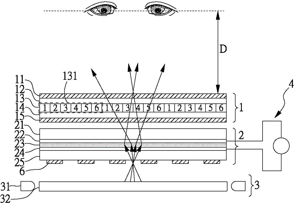
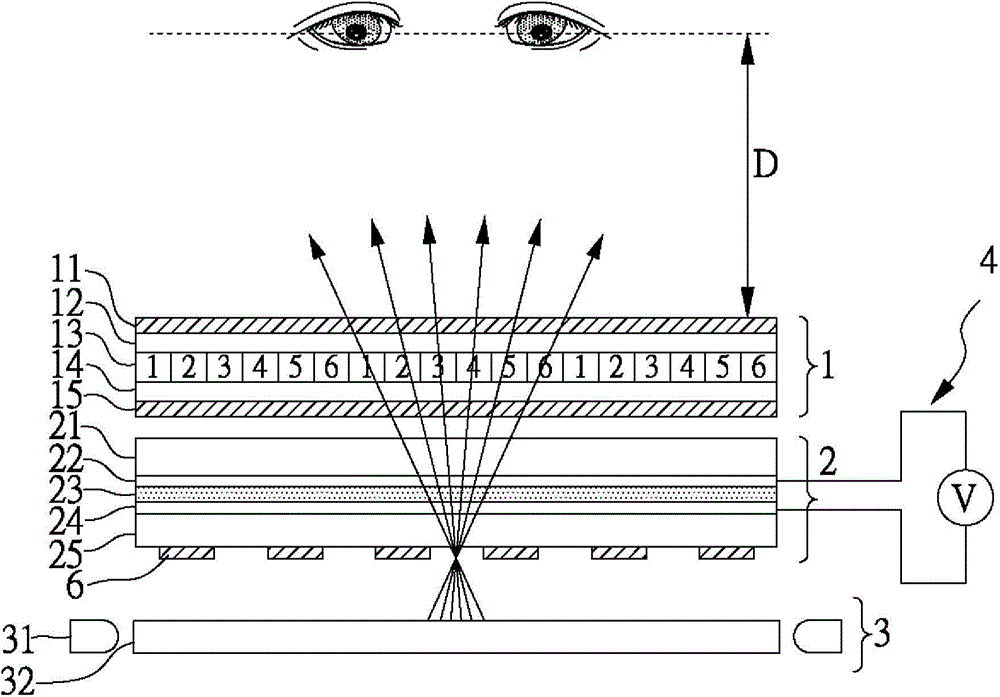
[0051] Please refer to Figure 1A , which is a schematic diagram of the display device of the present invention. The display device includes: a display unit 1 , a modulation unit 2 , and a backlight unit 3 , and the modulation unit 2 is arranged between the display unit 1 and the backlight unit 3 . The display unit 1 includes in sequence: a first polarizer 11, a first substrate 12, a pixel layer 13, a second substrate 14, and a second polarizer 15; the modulation unit 2 includes in sequence: a third substrate 21, a first conductive layer 22, liquid crystal layer 23, second conductive layer 24, fourth substrate 25, and barrier layer 6;
[0052]In the present invention, the display unit 1 is not limited, for example, it may be a common liquid crystal display unit (LCD) or an organic light emitting diode display unit (OLED). The pixel layer 13 includes a plurality of pixel units 131. When the display unit 1 is a liquid crystal display unit, the plurality of pixel units 131 inclu...
Embodiment 2
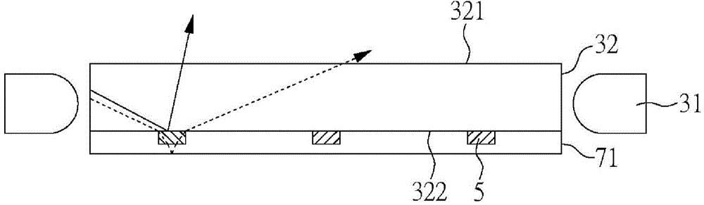
[0067] A detailed description of the backlight unit in the display device of the present invention is as follows. See Figure 2A , Figure 2B , which are two implementations in which multiple stripe patterns 5 and reflective layers 71 and 72 are provided on the backlight unit 3 . Wherein, the backlight unit 3 includes a light-emitting element 31 and a light guide plate 32, the light-emitting element 31 is arranged on both sides (light-incident surfaces) of the light-guide plate 32, and the light-guide plate has a first surface 321 (light-emitting surface) and an opposite second surface 322 (bottom surface), and the first surface 321 is adjacent to the modulation unit (not shown), and the second surface 322 of the light guide plate 32 is provided with a plurality of stripe patterns 5; as Figure 2A As shown, the reflective layer 71 can be disposed on the second surface 322 and cover the second surface 322 and the plurality of stripe patterns 5; or as Figure 2B As shown, the...
Embodiment 3
[0071] See image 3 , which is a schematic diagram of a display device in another embodiment of the present invention; in this embodiment, the display unit 1 is combined with the modulation unit 2 so that a substrate can be omitted. In detail, the display unit 1 includes in sequence: a first polarizer 11 , the first substrate 12, the pixel layer 13, and the second substrate 14, the modulation unit 2 includes in sequence: a first conductive layer 22, a liquid crystal layer 23, a second conductive layer 24, a fourth substrate 25, and a second polarizer Component 15; accordingly, the display unit 1 and the modulation unit 2 share the second substrate 14, and the third substrate 21 included in the modulation unit 2 in Embodiment 1 can be omitted, reducing the weight of the device and the cost of the substrate. In addition, the backlight unit 3 in this embodiment and Figure 2A Same, no longer repeat the description here.
[0072] In this embodiment, the display unit 1 is a liqui...
PUM
 Abstract
Description
Claims
Application Information
 - R&D
- Intellectual Property
- Life Sciences
- Materials
- Tech Scout
- Unparalleled Data Quality
- Higher Quality Content
- 60% Fewer Hallucinations
Browse by: Latest US Patents, China's latest patents, Technical Efficacy Thesaurus, Application Domain, Technology Topic, Popular Technical Reports.
© 2025 PatSnap. All rights reserved.Legal|Privacy policy|Modern Slavery Act Transparency Statement|Sitemap|About US| Contact US: help@patsnap.com