Early-stage detecting system and method for silicon chip electrical test

A silicon chip and electrical technology, applied in the field of early detection system of silicon chip electrical test, can solve the problem that WAT test data analysis cannot detect electrical performance in time, and solve the untimely nature of manual inspection, simple structure and steps , the effect of saving time

Active Publication Date: 2015-09-30
SEMICON MFG INT (SHANGHAI) CORP
View PDF3 Cites 6 Cited by
  • Summary
  • Abstract
  • Description
  • Claims
  • Application Information

AI Technical Summary

Problems solved by technology

[0005] In view of the shortcomings of the prior art described above, the purpose of the present invention is to provide an early detection system and method for electrical testing of silicon wafers, which is used to solve the problem that the analysis of WAT test data in the prior art cannot detect electrical properties in time

Method used


Image

  • Early-stage detecting system and method for silicon chip electrical test
  • Early-stage detecting system and method for silicon chip electrical test
  • Early-stage detecting system and method for silicon chip electrical test

Examples


Embodiment 1

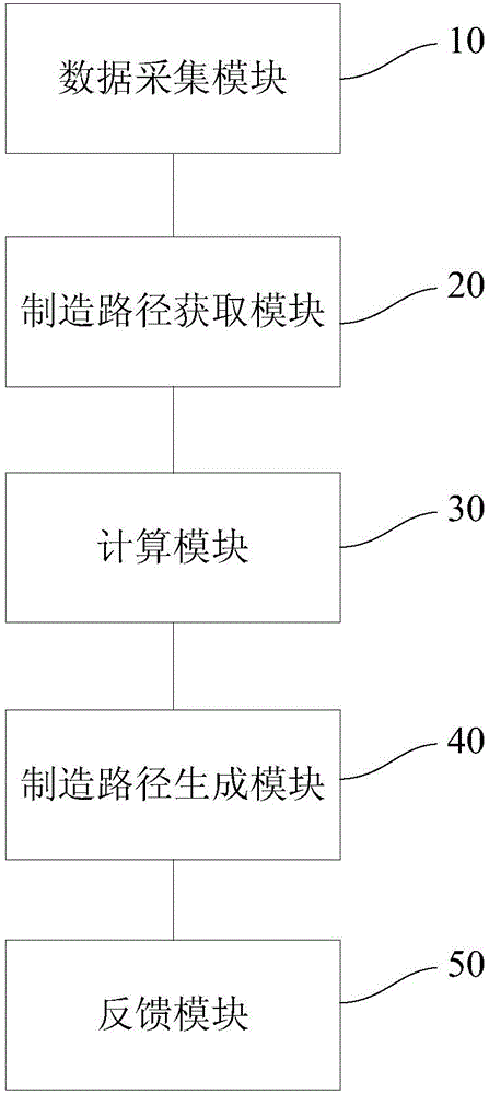
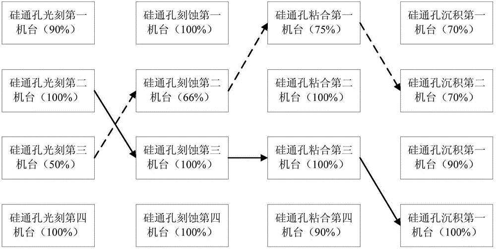
[0033] like figure 1 and image 3 As shown, this embodiment provides an early detection system for electrical testing of silicon wafers, including:

[0034] The data collection module 10 is used to collect silicon wafer electrical test data, and determine normal silicon wafers and abnormal silicon wafers based on the test data;

[0035] The manufacturing path acquisition module 20 is used to acquire the manufacturing paths of each of the normal silicon wafers and each of the abnormal silicon wafers in the process machine matrix;

[0036] The calculation module 30 is used to calculate the normal silicon wafer pass rate and abnormal silicon wafer pass rate of each process machine in the process machine matrix according to the manufacturing path;

[0037]The manufacturing path generation module 40 is used for generating a suitable manufacturing path for silicon wafers according to the normal silicon wafer throughput rate and the abnormal silicon wafer throughput rate.

[0038]...

Embodiment 2

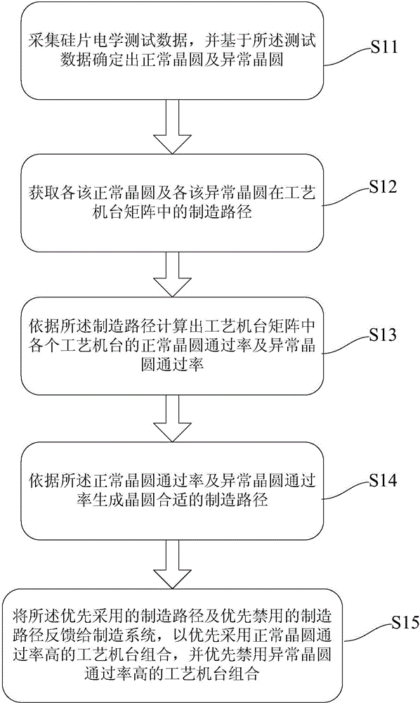
[0047] like figure 2 and image 3 As shown, this embodiment provides an early detection method for electrical testing of silicon wafers, including steps:

[0048] like figure 2 As shown, step 1) S11 is first performed to collect electrical test data of silicon wafers, and determine normal silicon wafers and abnormal silicon wafers based on the test data.

[0049] As an example, the silicon wafer electrical test data uses some special parameter test structures to replace products for current, voltage and capacitance tests to determine the silicon wafer electrical performance. The special parameter test structures include transistors, various line widths, Resistivity structure, capacitance structure, contact hole, via chain, meander structure, frame-in-frame structure, can be used to test resistance, voltage, capacitance, current and open circuit or short circuit test. .

[0050] As an example, this step uses a comparison method based on the test data to determine normal s...


PUM


Abstract

The invention provides an early-stage detecting system and method for a silicon chip electrical test. The early-stage detecting system includes a data collecting module used for collecting silicon chip electrical test data and determining normal silicon chips and abnormal silicon chips based on the test data; a making path acquiring module used for acquiring making paths of the normal silicon chips and the abnormal silicon chips in a processing platform matrix; a calculating module used for calculating normal silicon chip passing rate and abnormal silicon chip passing rate of each processing platform in the processing platform matrix according to the making paths; a making path generating module used for generating making paths suitable for silicon chips according to the normal silicon chip passing rates and the abnormal silicon chip passing rates. By adopting the system and method provided by the invention, making paths without abnormalities can be selected automatically. At the same time, processing platforms with poor performance can be denied. Therefore, timelessness of manual check performed by technique integration engineers is avoided and time for data analysis is saved.

Description

technical field [0001] The invention belongs to the field of semiconductor electrical qualification testing and testing, in particular to an early detection system and method for electrical testing of silicon wafers. Background technique [0002] Wafer Acceptance Test (WAT, Wafer Acceptance Test) is regarded as the last line of defense before silicon wafers leave the factory, and the quality and stability of silicon wafers can be guaranteed to a certain extent under the WAT test, and defective silicon wafers will not be damaged. will be sent to the customer. The main purpose of WAT is to simulate the circuit designed by customers, monitor the stability of Fab process and improve product yield, so WAT plays a very important role in IC design. For ICs, the basic electrical parameters, such as the measurement of MOS characteristics, resistance, etc., are the basic indicators to ensure whether the IC can operate normally. Therefore, under the condition that the measured basic ...

Claims


Application Information

Patent Timeline
Patent Type & Authority Applications(China)
IPC IPC(8): H01L21/66
CPCH01L22/12H01L22/14
Inventor 包巧霞余志贤
Owner SEMICON MFG INT (SHANGHAI) CORP
Why Eureka
Try Eureka