Multi-element photoelectric sensor
A photoelectric sensor and multiple technologies, applied in the fields of sensors, medical science, diagnostic recording/measurement, etc., can solve the problems of unsatisfactory detection accuracy and sensitivity of optical methods, and no single blood sugar, so as to avoid infection and reduce pain.
- Summary
- Abstract
- Description
- Claims
- Application Information
AI Technical Summary
Problems solved by technology
Method used
Image
Examples
Embodiment Construction
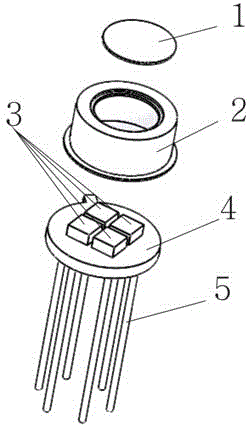
[0013] Such as figure 1 The multi-element photoelectric sensor shown includes a light guide 1, an upper shell 2 and a tube socket 4. The upper end surface of the tube socket 4 is fixedly connected with four photoelectric chips 3, and the upper shell 2 is fixedly connected to the tube socket 4 On the upper end surface, the light guide body 1 is fixedly connected to the upper shell 2, and the bottom of the tube socket 4 is connected with a pin 5, and the pin 5 is separately led from the anodes of the four photoelectric chips 3 and the four photoelectric chips The cathode of 3 is connected to one body, and the upper shell 2 is drawn out through the tube socket 4. The upper shell 2 is provided with a groove for the light guide 1 to be embedded, and the four photoelectric chips 3 are in the shape of "well" The four photoelectric chips 3 have receiving wavelengths of 416nm, 660nm, 940nm and 1025nm, respectively, and the light guide bandpass width of the light guide body 1 is 250nm-25...
PUM
 Abstract
Description
Claims
Application Information
