
Solid state imaging device, manufacturing method of the same, and electronic equipment

一种固态成像器件、成像的技术,应用在电固体器件、半导体器件、电视等方向,能够解决混色和色差、颜色不均匀等问题,达到抑制混色、抑制灵敏度降低的效果

Inactive Publication Date: 2015-10-07
SONY CORP
View PDF14 Cites 23 Cited by
  • Summary
  • Abstract
  • Description
  • Claims
  • Application Information

AI Technical Summary

Problems solved by technology

[0007] However, there are cases where, when the arrangement pitch between color filters is narrow, color mixing and chromatic aberration (color unevenness) occur due to process differences due to displacement occurring during alignment of the photolithography process of the color filters. )

Method used


Image

  • Solid state imaging device, manufacturing method of the same, and electronic equipment
  • Solid state imaging device, manufacturing method of the same, and electronic equipment
  • Solid state imaging device, manufacturing method of the same, and electronic equipment

Examples


Embodiment Construction

[0097]

[0098] (Configuration example of illustrative embodiment of solid-state imaging device)

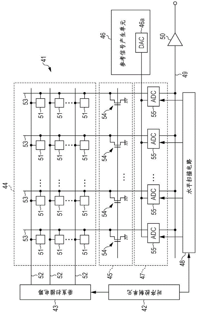
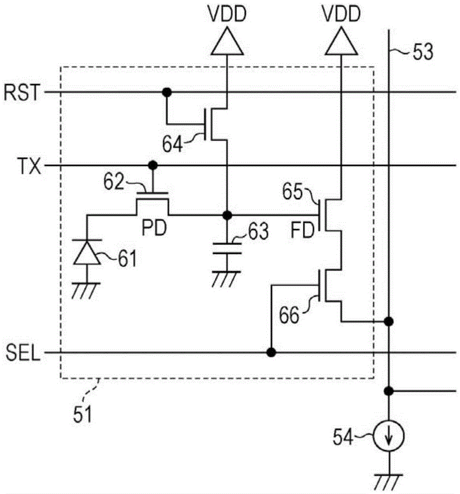
[0099] figure 1 is a block diagram showing an illustrative configuration example of an embodiment of a solid-state imaging device to which the present invention is applied.

[0100] figure 1 The solid-state imaging device 41 is configured to include a timing control unit 42 on a semiconductor substrate (not shown), a vertical scanning circuit 43, a pixel array unit 44, a constant current source circuit unit 45, a reference signal generation unit 46, a column AD conversion unit 47 . Horizontal scanning circuit 48 , horizontal output line 49 and output circuit 50 .

[0101] The timing control unit 42 supplies clock signals or timing signals necessary for predetermined operations to the vertical scanning circuit 43 and the horizontal scanning circuit 48 on the basis of a master clock of a predetermined frequency. For example, the timing control unit 42 supplies a timing signal ...


PUM


Abstract

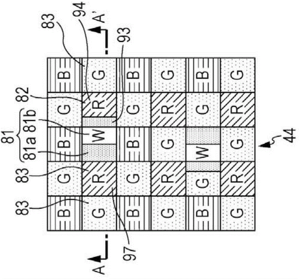
A solid state imaging device that includes a phase difference detection pixel which is a pixel for phase difference detection; a first imaging pixel which is a pixel for imaging and is adjacent to the phase difference detection pixel; and a second imaging pixel which is a pixel for imaging other than the first imaging pixel. An area of a color filter of the first imaging pixel is smaller than an area of a color filter of the second imaging pixel.

Description

technical field [0001] The present invention relates to a solid-state imaging device, a method of manufacturing the solid-state imaging device, and electronic equipment. In particular, the present invention relates to a solid-state imaging device, a manufacturing method of the solid-state imaging device, and an electronic device capable of suppressing color mixing and sensitivity reduction in pixels for phase difference detection. [0002] Cross References to Related Applications [0003] This application claims the priority of Japanese priority patent application JP2013-257294 filed on December 12, 2013 and Japanese priority patent application JP2014-109412 filed on May 27, 2014, and the above Japanese priority application The entire content of is incorporated herein by reference. Background technique [0004] In recent years, imaging devices such as digital still cameras and digital video cameras that image subjects such as humans or animals and record image data obtaine...

Claims


Application Information

Patent Timeline
Patent Type & Authority Applications(China)
IPC IPC(8): H04N5/374H01L27/146
CPCH01L27/14623H01L27/14818H01L27/14607H01L27/14612H01L27/14621H01L27/14634H01L27/14645H01L27/14685H01L27/14689H04N25/76H04N9/01H04N25/75
Inventor 田舎中博士井上裕士中田征志
Owner SONY CORP
Learn More