Display panel of conductive layer with variable line widths
A display panel and conductive layer technology, applied in nonlinear optics, instruments, optics, etc., can solve problems such as poor design of display panels, reduced reliability, and decreased panel yield
- Summary
- Abstract
- Description
- Claims
- Application Information
AI Technical Summary
Problems solved by technology
Method used
Image

Examples
no. 1 example
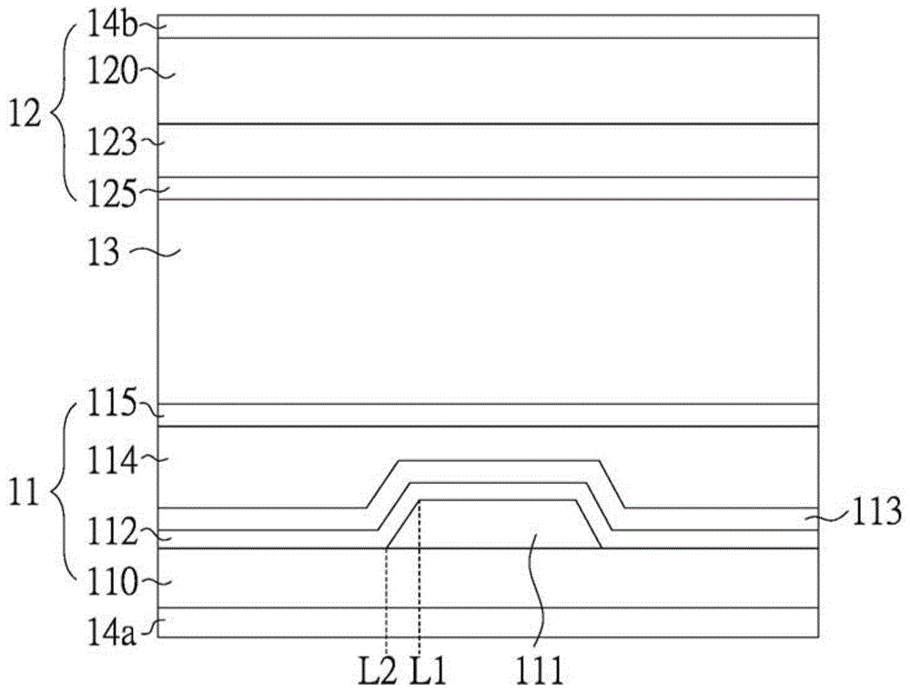
[0059] figure 2 A partial side view of a conductive layer of a display panel according to the first embodiment of the present invention is briefly shown. It should be noted that although the variation of the line width of the second conductive layer is used as an example for illustration in the embodiment, the present invention is not limited thereto, and the design of the embodiment can also be applied to other conductive layers without departing from the spirit of the present invention. . Furthermore, on the basis of knowledge that can be fully understood by those skilled in the art, only relevant elements are simply drawn in the diagrams to clearly illustrate the embodiments of the present invention.
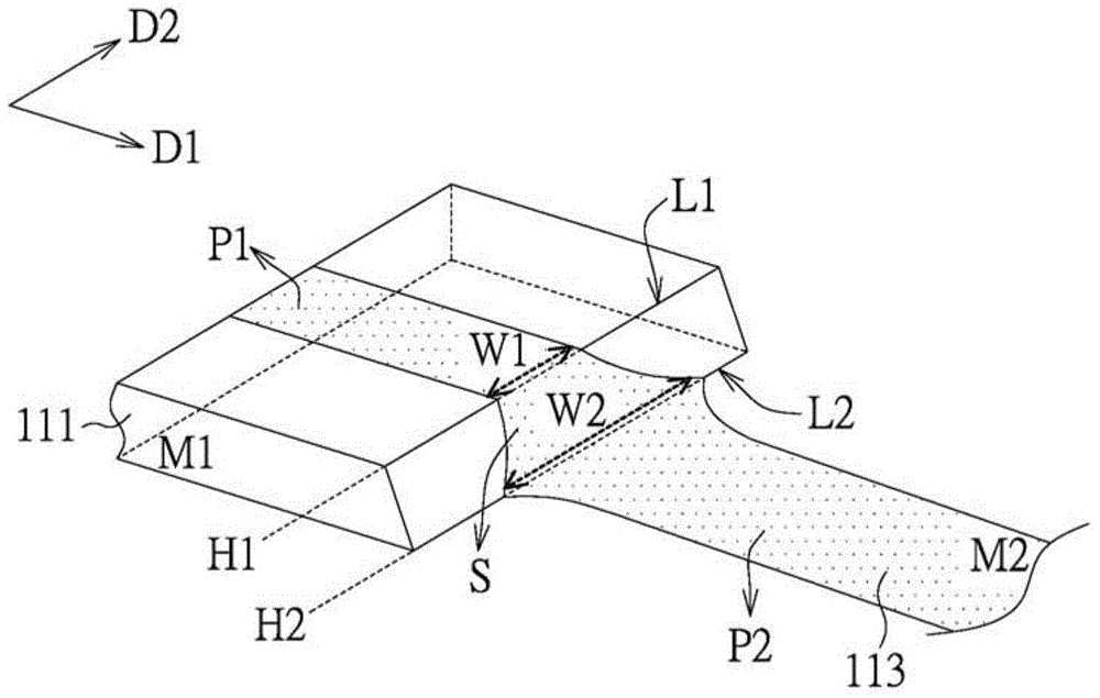
[0060] In one embodiment, a conductive layer on a substrate, such as the second conductive layer ( M2 ) 113 of the first substrate 11 , extends along a first direction D1 . The second conductive layer 113 along the first direction D1 is sequentially a first plane P1 at a f...
no. 2 example
[0071] Figure 4 A partial side view schematically showing a conductive layer of a display panel according to a second embodiment of the present invention. Same as the first embodiment, in the second embodiment, the change of the line width of the second conductive layer 113' across the first conductive layer 111' is also used as an example for illustration, but the present invention is not limited thereto.
[0072] Please also refer to figure 1 . Same as the first embodiment, a conductive layer on a substrate in the second embodiment, such as the second conductive layer (M2) 113' of the first substrate 11, extends along a first direction D1, and the first conductive layer 111' extends along the The second direction D2 extends, and the second direction D2 is perpendicular to the first direction D1. The first plane P1 of the second conductive layer 113' corresponds to the top surface of the first conductive layer 111', the second plane P2 of the second conductive layer 113' ...
no. 3 example
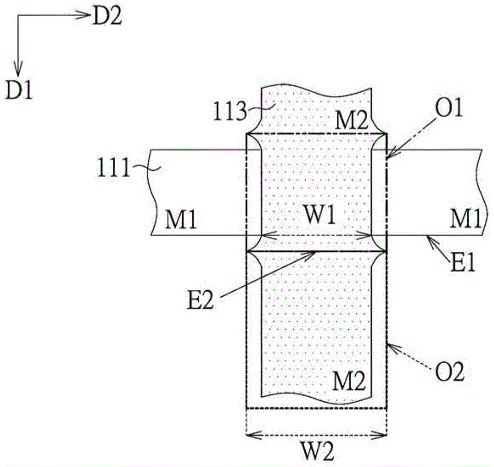
[0083] Figure 6 A partial top view of a conductive layer in a display panel according to a third embodiment of the present invention is briefly shown. In the third embodiment, an example in which the second conductive layer M2 crosses a gate line (Gate line) and a common line Com (common line) is used for illustration. But the present invention is not limited to Figure 6 However, it is possible to make appropriate changes and adjustments according to the actual application conditions.
[0084] In the third embodiment, it is also assumed that the slope of the gate line Gate and the common line Com is relatively steep, and the two boundaries formed by the top surface and the bottom surface are almost superimposed into the same line segment in the upper view, as shown in Figure 5B shown.
[0085] In the third embodiment, the line width design as shown in the second embodiment is adopted, for example: the higher part of the second conductive layer M2 (i.e. the area overlappi...
PUM
 Abstract
Description
Claims
Application Information
 - R&D
- Intellectual Property
- Life Sciences
- Materials
- Tech Scout
- Unparalleled Data Quality
- Higher Quality Content
- 60% Fewer Hallucinations
Browse by: Latest US Patents, China's latest patents, Technical Efficacy Thesaurus, Application Domain, Technology Topic, Popular Technical Reports.
© 2025 PatSnap. All rights reserved.Legal|Privacy policy|Modern Slavery Act Transparency Statement|Sitemap|About US| Contact US: help@patsnap.com