RF switch circuit
A technology of switching circuits and switches, applied in the direction of circuits, electronic switches, electrical components, etc.
- Summary
- Abstract
- Description
- Claims
- Application Information
AI Technical Summary
Problems solved by technology
Method used
Image

Examples
Embodiment Construction
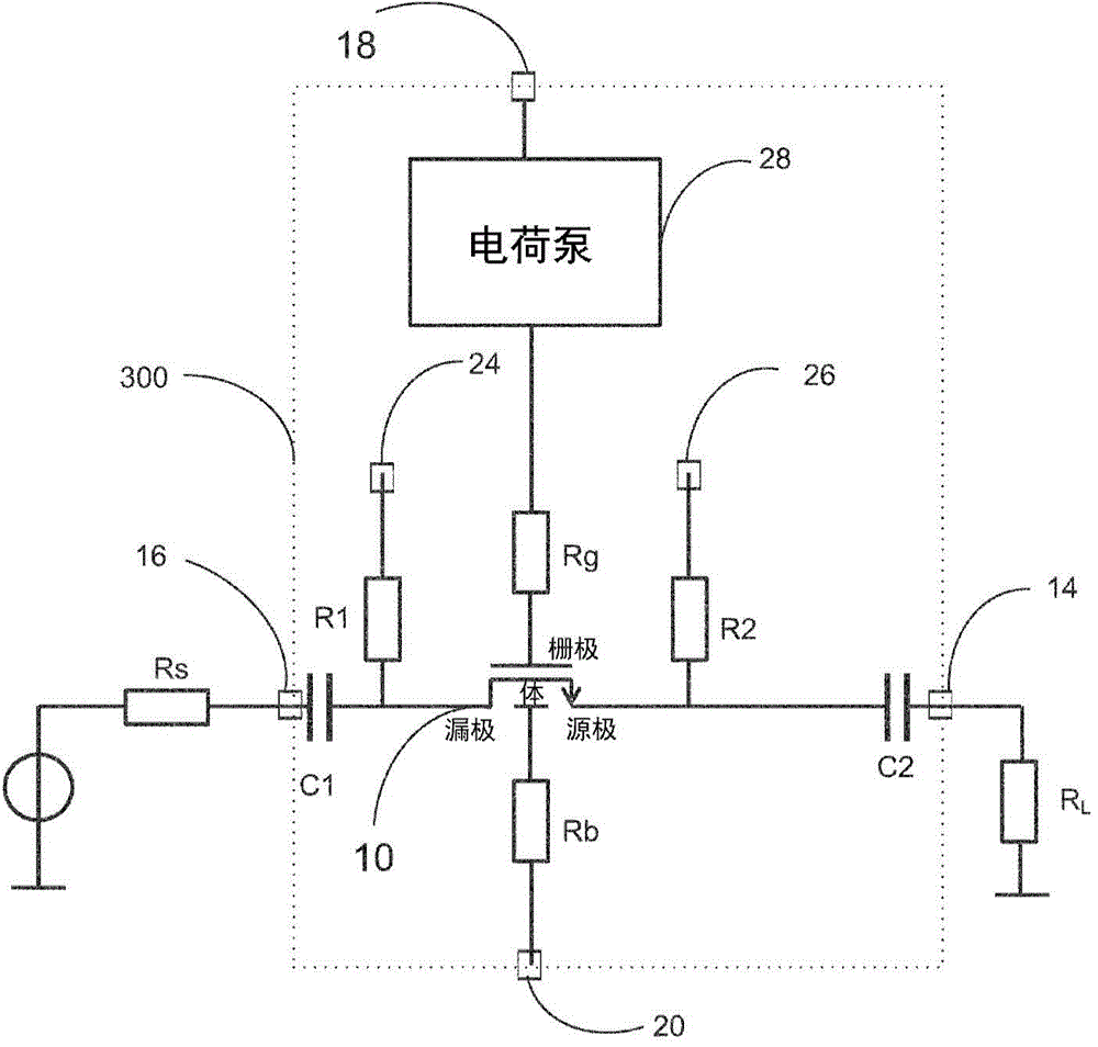
[0041] Figure 4 An RF switch circuit 400 is shown. A first resistor R1 may be connected between a drain of the NMOS transistor 10 and an output of a bias swap circuit 30 . The second resistor R2 may be connected between the source of the NMOS transistor 10 and the output of the bias switching circuit 30 . A decoupling capacitor C1 may be connected between the drain of the NMOS transistor 10 and the RF input 16 of the RF switch. A decoupling capacitor C2 may be connected between the source of NMOS transistor 10 and RF output 14 . A bootstrap gate resistor Rg may be connected between the control input 18 and the control terminal or gate of the NMOS 10 . The body bias resistor Rb may be connected to a bias voltage supply rail, which may be at ground potential.
[0042] In operation, the RF input 16 may be connected to an RF signal source with source impedance Rs. The RF signal source may be, for example, an RF power amplifier or an antenna. An RF switch RF output 14 may be...
PUM
 Abstract
Description
Claims
Application Information
 - Generate Ideas
- Intellectual Property
- Life Sciences
- Materials
- Tech Scout
- Unparalleled Data Quality
- Higher Quality Content
- 60% Fewer Hallucinations
Browse by: Latest US Patents, China's latest patents, Technical Efficacy Thesaurus, Application Domain, Technology Topic, Popular Technical Reports.
© 2025 PatSnap. All rights reserved.Legal|Privacy policy|Modern Slavery Act Transparency Statement|Sitemap|About US| Contact US: help@patsnap.com