Circuit for high-resolution phase detection in a digital RF processor

a phase detection and phase detection technology, applied in the field of data communication, can solve the problems of less than ideal, limited buffer delay in the minimum time resolution of these prior art designs, and the above approaches, so as to reduce power consumption and be less sensitive

Active Publication Date: 2007-04-17
TEXAS INSTR INC
View PDF2 Cites 109 Cited by
  • Summary
  • Abstract
  • Description
  • Claims
  • Application Information

AI Technical Summary

Benefits of technology

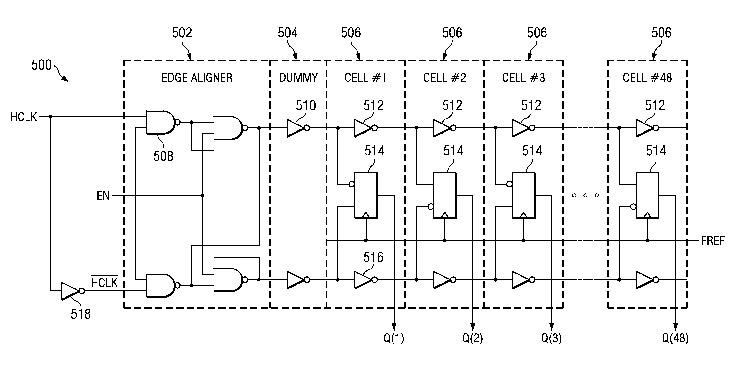
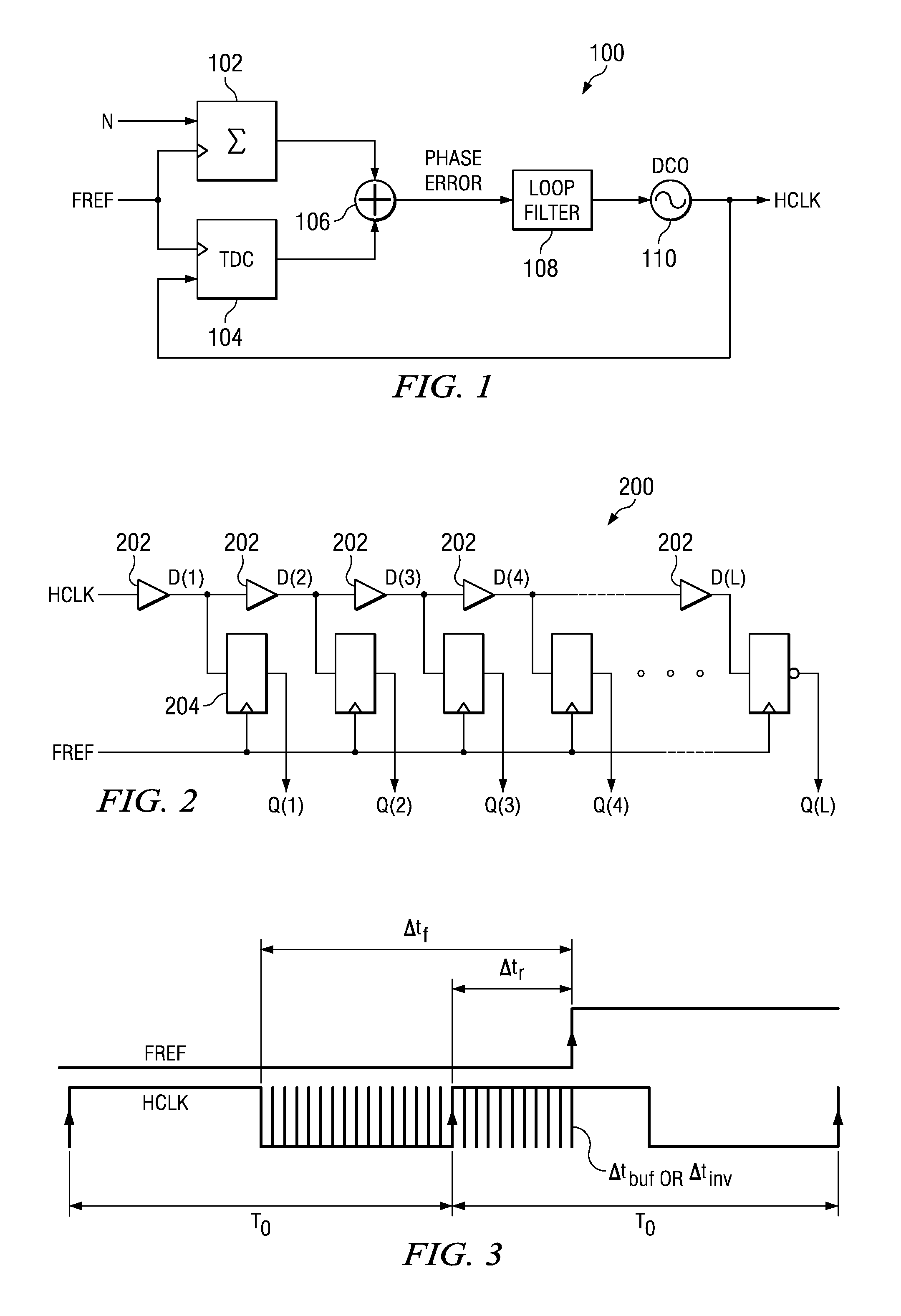
[0006]The present invention provides a solution to the problems of the prior art by providing a novel time-to-digital converter (TDC) based on a pseudo-differential digital architecture. The TDC circuit architecture can be used as a phase / frequency detector and charge pump replacement in an all-digital PLL within a digital radio transceiver. The pseudo-differential digital architecture of the TDC circuit makes it less sensitive to NMOS and PMOS transistor mismatches. The time conversion resolution is equal to an inverter propagation delay, for example 15–20 ps, depending on the particular process. The inverter propagation delay is the finest logic-level regenerative timing in CMOS. In addition, the TDC circuit of the present invention is self-calibrating, with the estimation accuracy better than 1%, in order to produce the output that is independent from process, voltage and temperature variations. The output could be normalized to a period of the high frequency clock input. The TDC circuit can also serve as a CMOS inverter delay indicator for the purpose of inverter delay normalization, thus also providing an indication of process strength for analog circuits in large system on chip (SoC) dies. The TDC circuit also incorporates power management circuitry to significantly reduce power consumption to a very low level.
[0007]The TDC architecture of the present invention takes advantage of the deep-submicron CMOS process strengths of ultra-fast logic switching while avoiding its weaker handling of voltage resolution. It is recognized that an inverter propagation delay is the finest logic-level regenerative timing method in CMOS. To this extent, the invention avoids any control of the inverter delay that would make it slower, such as using current starving techniques or increasing capacitative loads. To maximize performance, the invention also avoids fully differential structures that would require current biasing. The resolution of the TDC circuit of the present invention is the fastest possible intrinsic inverter delay (e.g., 15–20 ps in the particular CMOS process used).
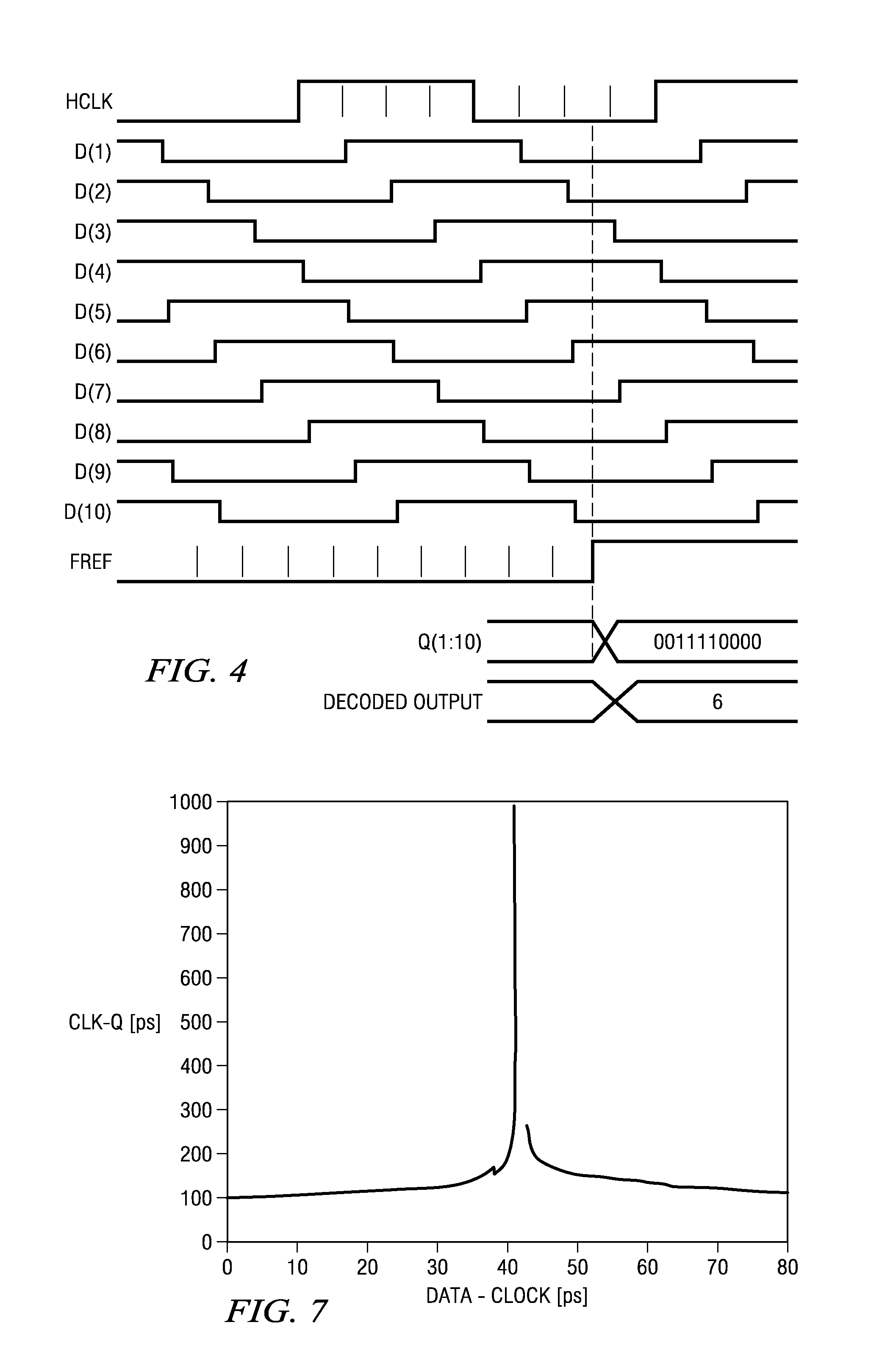
[0009]The TDC core comprises of inverters and flip-flops and does not require any current biasing, analog interpolation or precise scaling of sub-gate delays. The architecture is based on a pseudo-differential topology that makes it less sensitive to differing strengths of NMOS and PMOS transistors. This brings the TDC resolution down to the intrinsic delay of the inverter, instead of the buffer, as in prior art designs. Taking advantage of the availability of the two opposite phase clocks (or one clock with an opposite phase generated internally), a novel all-digital calibration method of an inverter delay could be run during the normal operation to compensate for temperature and voltage drifts. Since the calibration circuit reports a delay of an intrinsic, uncorrected inverter in digital form, it can be used as a CMOS process strength indicator for process statistics and to calibrate bias current of other analog circuits on the same die. A novel power management scheme through dynamic clock gating is applicable in PLL and other applications where the time-of arrival can be predicted. The TDC has been realized and its resolution has been measured to be as low as 17–21 ps with integral nonlinearity (INL) of 0.7 LSB. This is achieved with very low power consumption and area usage.
[0011]The TDC of the present invention, offers significantly better performance compared to previously known solutions: (1) 2–3 times lower phase error in the transmitter, (2) highly linear TDC with 30%–50% better linearity than previous solutions, (3) 2 times improvement in resolution for phase detection, and (4) uniform performance across all channels and multiple radio bands. The above described differences contribute to a multi-band RF transceiver supporting low phase noise requirements for standards such as GSM.
[0012]The advantages of the present invention include: (1) accurate phase detection with <0.5 LSB INL / DNL and high-resolution of 20 ps, (2) faster lock and PLL settling times, (3) very low power consumption fractional phase detection circuit (less than 0.5 mW), (4) very small area (0.01 mm2) phase detection circuit, and (5) glitch / error free TDC output digital code resulting in faster acquisition and PLL settling times.

Problems solved by technology

The minimum time resolution of these prior art designs, however, is limited to a buffer delay.
The above approaches, however, are less than ideal since they are analog intensive, require extensive calibration for high-volume production, suffer from long dead time and large power dissipation and require relatively large silicon area.

Method used


Image

  • Circuit for high-resolution phase detection in a digital RF processor
  • Circuit for high-resolution phase detection in a digital RF processor
  • Circuit for high-resolution phase detection in a digital RF processor

Examples


Embodiment Construction

Notation Used Throughout

[0038]The following notation is used throughout this document.

[0039]

TermDefinitionADCAnalog to Digital ConverterADPLLAll Digital Phase Locked LoopASICApplication Specific Integrated CircuitCMOSComplementary Metal Oxide SemiconductorDBBDigital BasebandDCODigitally Controlled OscillatorDCXODigitally Controlled Crystal OscillatorDLLDelay Locked LoopDNLDifferential NonlinearityDPADigital Power AmplifierDRPDigital RF Processor or Digital Radio ProcessorDSPDigital Signal ProcessorEDGEEnhanced Data rates for Global EvolutionFOMFigure-of-MeritFPGAField Programmable Gate ArrayFREFFrequency ReferenceGSMGlobal System for Mobile CommunicationHDLHardware Description LanguageICIntegrated CircuitINLIntegral NonlinearityLANLocal Area NetworkLDOLow DropoutLSBLeast Significant BitMOSMetal Oxide SemiconductorNMOSn-channel Metal Oxide SemiconductorPLLPhase Locked LoopPMPower ManagementPMOSp-channel Metal Oxide SemiconductorPVTProcess Voltage TemperatureRFRadio FrequencyRFBISTRF ...


PUM


Abstract

A novel time-to-digital converter (TDC) used as a phase / frequency detector and charge pump replacement in an all-digital PLL within a digital radio processor. The TDC core is based on a pseudo-differential digital architecture making it insensitive to NMOS and PMOS transistor mismatches. The time conversion resolution is equal to an inverter propagation delay, e.g., 20 ps, which is the finest logic-level regenerative timing in CMOS. The TDC is self calibrating with the estimation accuracy better than 1%. The TDC circuit can also serve as a CMOS process strength estimator for analog circuits in large SoC dies. The circuit also employs power management circuitry to reduce power consumption to a very low level.

Description

REFERENCE TO RELATED APPLICATIONS[0001]This application claims priority to U.S. Provisional Application Ser. No. 60 / 629,829, filed Nov. 18, 2004, entitled “A Circuit for High-Resolution Phase Detection in a Digital Radio Transceiver”, incorporated herein by reference in its entirety.FIELD OF THE INVENTION[0002]The present invention relates to the field of data communications and more particularly relates to time-to-digital converter with a pseudo-differential circuit architecture for precise phase detection incorporating a phase aligner and power management.BACKGROUND OF THE INVENTION[0003]Time-to-digital converters (TDC) are well known in the prior art. TDC circuits are currently widely used for time interval measurements in applications such as space science, high-energy physics, laser range finders and in test instrumentation. Recently, TDC circuits have been applied to frequency synthesis in delay locked loops (DLLs) to achieve faster acquisition and to avoid false locking. With...

Claims


Application Information

Patent Timeline
Patent Type & Authority Patents(United States)
IPC IPC(8): H03M1/50
CPCG04F10/005H03L7/091H04L27/361
Inventor VEMULAPALLI, SUDHEER K.WALLBERG, JOHNVALLUR, PRASANT K.STASZEWSKI, ROBERT B.
Owner TEXAS INSTR INC
Why Eureka
Try Eureka