Phase-locked loop circuit and delay-locked loop circuit

a phase-locked loop and delay-locked technology, applied in the direction of phase difference detection angle demodulation, automatic control of pulses, electrical devices, etc., can solve the problem of difficult circuit design to correct exactly 100% of jitter, rectangular waveform of control voltage of voltage controlled oscillator or voltage controlled delay circuit ends up being blunted, etc. problem, to achieve the effect of reducing frequency change and reducing frequency chang

Inactive Publication Date: 2005-10-11
SONY CORP
View PDF10 Cites 115 Cited by
  • Summary
  • Abstract
  • Description
  • Claims
  • Application Information

AI Technical Summary

Benefits of technology

[0120]An object of the present invention is to provide a phase-locked loop circuit and a delay-locked loop circuit able to reduce frequency change due to noise and able to reduce frequency change after a phase pull-in operation performed in each cycle of a reference clock signal.

Problems solved by technology

However, digital noise generated in shorter periods than that of the reference clock signal can be considered as random components in each cycle of the reference clock signal and cannot be corrected sufficiently by the feedback loop, thus causing jitter after the PLL is locked.
However, since the change of the voltage of the pulse signal input to a VCO circuit cannot be made too large during phase pull-in, it is difficult to design the circuit to correct exactly 100% of the jitter by the phase pull-in alone.
However, when a low-pass filter is provided after the lag-lead filter to reduce the influence of noise or when a capacitor is provided to stabilize the control voltage between an output of a bias circuit and a ground line or a power line, the rectangular waveform of the control voltage of a voltage controlled oscillator or a voltage controlled delay circuit ends up being blunted.
Therefore, there is a disadvantage that the effect of digital phase correction ends up declining at the trailing edge of the horizontal synchronization signal HSYNC, and the merit of using a lag-lead filter is lost.
In this case, however, it becomes difficult to satisfy equation (11).
That is, if the time constant τLP1 of the low-pass filter 104 is increased to reduce the influence of the noise, the control voltage continues changing even after the trailing edge of the reference clock signal φREF, so there arises a problem that the effect of the phase correction performed at the trailing edge of the reference clock signal φREF ends up being reduced.
However, when a large consumed power is injected into the above bias circuit 107, the overall power consumption of the PLL circuit ends up being increasingly increased, so usually the power consumption of the bias circuit 107 has to be kept lower than the power consumption of the voltage-controlled oscillator 105.
However, since the voltage of the bias voltage NBIAS decreases gradually, the voltage change of the bias voltage PBIAS gradually levels off.
That is, the bias voltage continues changing even after the trailing edge of the reference clock signal φREF, so there arises a problem that the effect of the phase correction performed at the trailing edge of the reference clock signal φREF ends up being reduced.

Method used


Image

  • Phase-locked loop circuit and delay-locked loop circuit
  • Phase-locked loop circuit and delay-locked loop circuit
  • Phase-locked loop circuit and delay-locked loop circuit

Examples


first embodiment

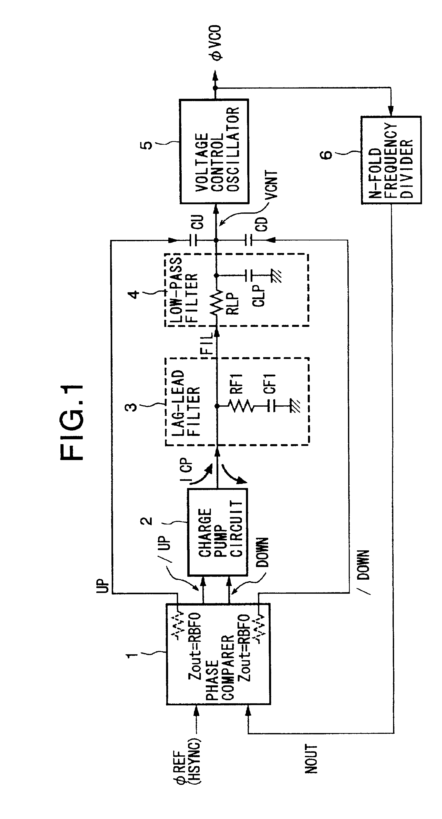
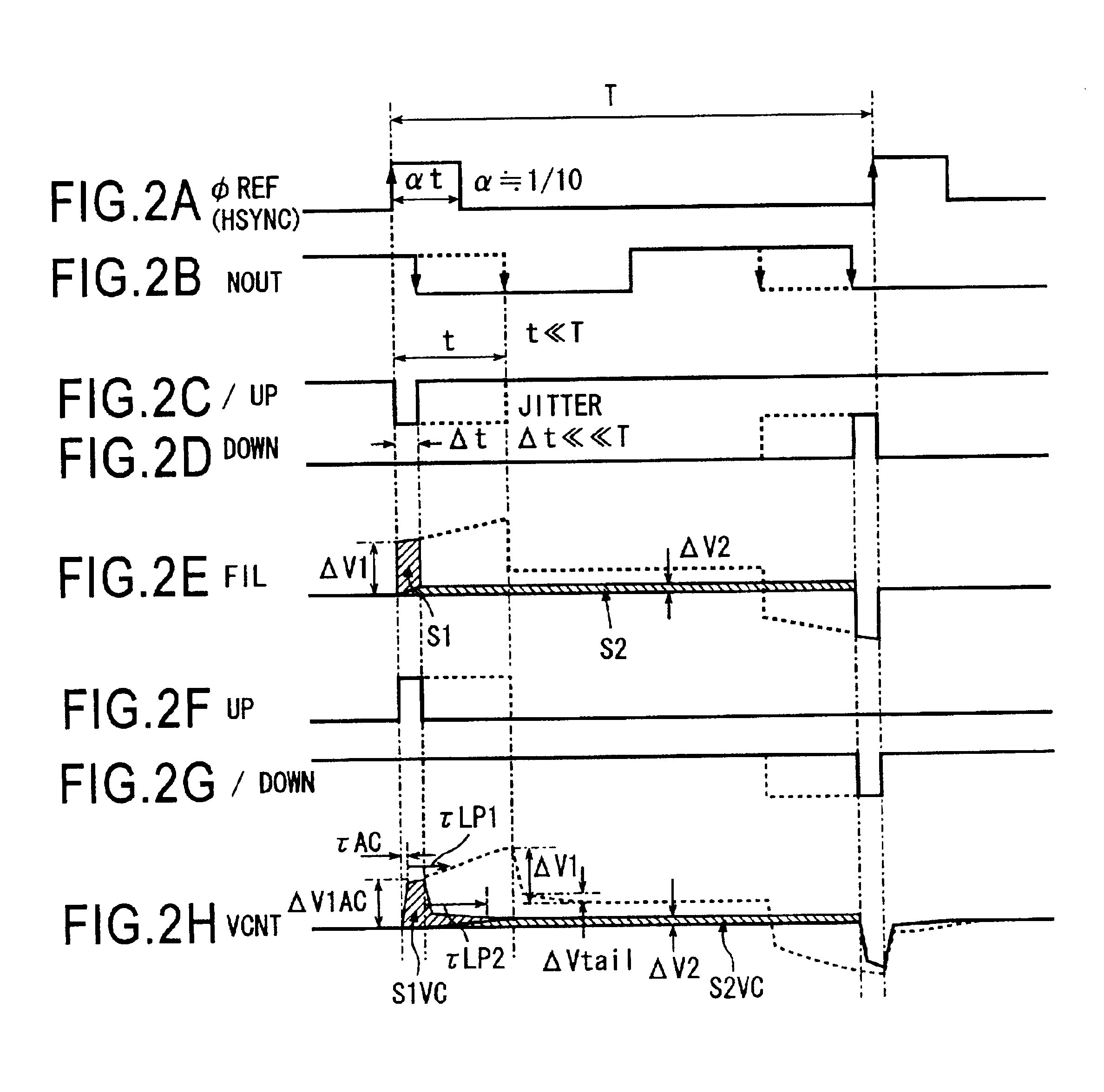
[0162]FIG. 1 is a view of the configuration of a first embodiment of a PLL circuit according to the present invention.

[0163]The PLL circuit shown in FIG. 1 includes a phase comparator 1, a charge pump circuit 2, a lag-lead filter 3, a low-pass filter 4, a voltage-controlled oscillator 5, a frequency divider 6, a capacitor CU, and a capacitor CD.

[0164]The phase comparator 1 compares phases of a reference signal φREF and an output signal NOUT of the frequency divider 6 and outputs an up signal and an inverted up signal / UP and a down signal and an inverted down signal / DOWN according to the result of comparison.

[0165]The charge pump circuit 2 receives the up signal / UP and the down signal DOWN from the phase comparator 1 and outputs a charging and discharging current ICP to the lag-lead filter 3.

[0166]The lag-lead filter 3, for example, is comprised of a resistor RF1 and a capacitor CF1 connected in series between the output of the charge pump circuit 2 and the ground line. It receive...

second embodiment

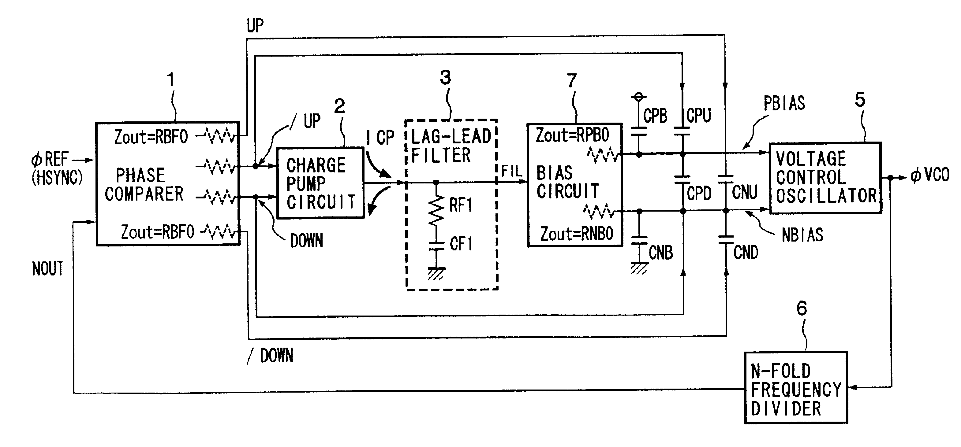
[0194]FIG. 3 is a view of the configuration of a second embodiment of a PLL circuit according to the present invention.

[0195]The PLL circuit shown in FIG. 3 includes a phase comparator 1, a charge pump circuit 2, a lag-lead filter 3, a bias circuit 7, a voltage-controlled oscillator 5, a frequency divider 6, a capacitor CPB, a capacitor CNB, a capacitor CPU, a capacitor CPD, a capacitor CNU, and a capacitor CND.

[0196]The same reference numerals in FIG. 3 and FIG. 1 refer to the same constituent elements.

[0197]The voltage-controlled oscillator 5 for example has a circuit as shown in FIG. 15 described above.

[0198]The bias circuit 7 for example has a circuit as shown in FIG. 16 described above.

[0199]The PLL circuit of the present invention shown in FIG. 3 differs from the PLL circuit of the prior art shown in FIG. 13 in the point that in the PLL circuit in FIG. 3, a capacitor CNU and a capacitor CND are provided on the output line of the bias voltage NBIAS, the outputs of the phase com...

third embodiment

[0215]FIG. 5 is a view of the configuration of a third embodiment of a PLL circuit according to the present invention.

[0216]The PLL circuit shown in FIG. 5 includes a phase comparator 1, a charge pump circuit 2, a lag filter 4, a voltage-controlled oscillator 5, a frequency divider 6, a capacitor CU, and a capacitor CD.

[0217]The same reference numerals in FIG. 5 and FIG. 1 refer to the same constituent elements.

[0218]The point of difference of the first embodiment of the present invention shown in FIG. 1 and the third embodiment of the present invention shown in FIG. 5 lies in the fact that the lag-lead filter 3 which had been inserted between the low-pass filter 4 and the charge pump 2 in the PLL circuit in FIG. 1 is deleted from the PLL circuit in FIG. 5.

[0219]In the PLL circuit in FIG. 5, a capacitor CU and a capacitor CD are provided at the output of the lag filter (low-pass filter) 4, and the outputs of the phase comparator 1, that is, the up signal UP and down signal / DOWN, ar...


PUM


Abstract

A PLL circuit and a DLL circuit able to stabilize a control voltage within a short time after a phase pull-in operation in each cycle of a reference clock. In a phase comparator, the size of a leading phase or a delayed phase of a feedback signal is detected with respect to a reference clock signa, and pulse signals having pulse widths corresponding to the size are output. A current corresponding to the signals is output from a charge pump circuit to a lag-lead filter, and a control voltage obtained by removing noise of the above output is output from a low-pass filter to a voltage-controlled oscillator. Furthermore, through capacitors, pulse signals are superposed on the control voltage, and a sharp waveform is obtained by correcting blunting of the waveform by the low-pass filter. Due to this, the control voltage is stabilized within a short time after a phase pull-in operation in each cycle of the reference clock signal.

Description

BACKGROUND OF THE INVENTION[0001]1. Field of the Invention[0002]The present invention relates to a phase-locked loop circuit and a delay-locked loop circuit, for example, and relates to a phase-locked loop circuit and a delay-locked loop circuit in a digital television set for generating dot clocks.[0003]2. Description of the Related Art[0004]For displaying a video signal on a display of a personal computer or for displaying OSD (on screen display) text on a television monitor, use is made of dot clocks obtained by multiplication by a PLL (phase-locked loop) circuit using the horizontal synchronization signal HSYNC as a reference clock signal. If the jitter of the PLL circuit is large, flicker or waving will appear on the screen and will end up being caught visually, so a PLL circuit having low jitter is considered necessary for a dot clock generating circuit.[0005]A change of voltage conditions slower than the reference clock signal or the natural frequency of a PLL circuit is corr...

Claims


Application Information

Patent Timeline
Patent Type & Authority Patents(United States)
IPC IPC(8): H03L7/18H03L7/08H03L7/089H03L7/107H03L7/093
CPCH03L2207/06H03L7/0891H03L7/0893H03L7/18H03L7/08
Inventor TACHIMORI, HIROSHI
Owner SONY CORP
Why Eureka
Try Eureka