
A far-field vector optical property modeling method for nanoscale 3D shape measurement

A technology of three-dimensional topography and modeling method, which is applied in the field of far-field vector optical characteristic modeling, which can solve the problem of lack of overall design of vector optical far-field modeling system, without considering a series of factors of high NA objective lens, and three-dimensional topography reconstruction. Insufficient information and other problems, to achieve the effect of improving the phenomenon of insufficient information and loss, easy control and strong applicability

Active Publication Date: 2017-09-01
HUAZHONG UNIV OF SCI & TECH
View PDF4 Cites 0 Cited by
  • Summary
  • Abstract
  • Description
  • Claims
  • Application Information

AI Technical Summary

Problems solved by technology

[0004] However, further research shows that the above-mentioned prior art still has the following defects or deficiencies: First, it does not make a more in-depth study of the entire process and propagation mechanism of the electromagnetic field distribution at the near field of the detection sample to the final detection plane. In particular, the lack of a more rigorous and accurate overall design of the vector optics far-field modeling system has led to insufficient and lost information on the 3D shape reconstruction of the final probed sample; secondly, the Mueller matrix, which includes More polarization information of the sample, the equipment used in the above-mentioned prior art often only obtains the information of the 0th order diffracted light or only obtains the electric field distribution at the entrance pupil of the high NA objective lens without considering a series of factors of the high NA objective lens, etc. Correspondingly, the available measurement information is relatively small; based on the above analysis, it is necessary to make further research and improvement in the field of nanoscale three-dimensional surface topography detection in order to better apply to microelectronic integrated circuits and microelectromechanical systems. high-precision applications such as

Method used


Image

  • A far-field vector optical property modeling method for nanoscale 3D shape measurement
  • A far-field vector optical property modeling method for nanoscale 3D shape measurement
  • A far-field vector optical property modeling method for nanoscale 3D shape measurement

Examples


Embodiment Construction

[0032] In order to make the object, technical solution and advantages of the present invention clearer, the present invention will be further described in detail below in conjunction with the accompanying drawings and embodiments. It should be understood that the specific embodiments described here are only used to explain the present invention, not to limit the present invention. In addition, the technical features involved in the various embodiments of the present invention described below can be combined with each other as long as they do not constitute a conflict with each other.

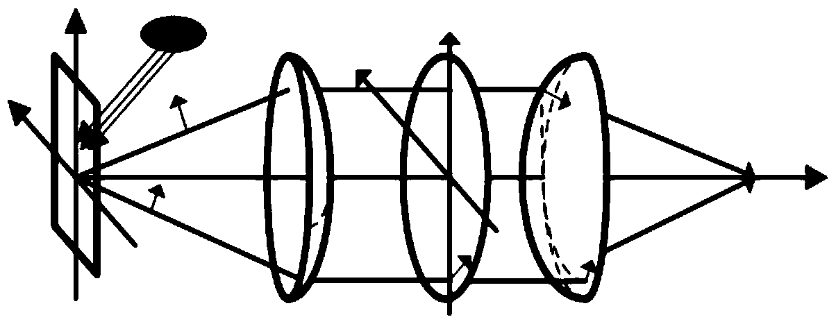
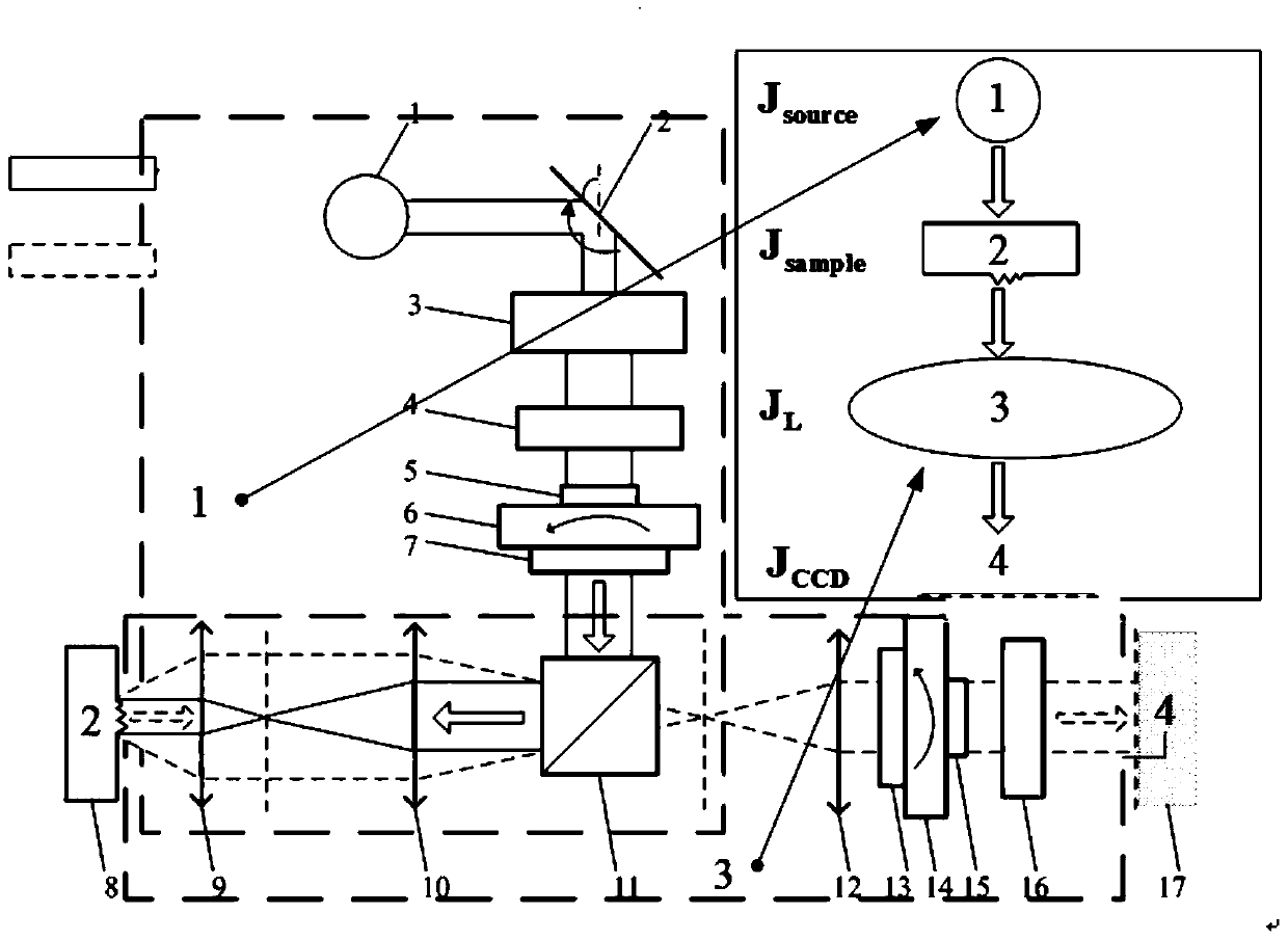
[0033] figure 1 It is an overall process flow chart of the far-field vector optical characteristic modeling method constructed according to the present invention. Such as figure 1 As shown in , the process flow mainly includes the following processing steps:

[0034] First, in Step 1, various conventional measuring instruments can be used to obtain the vector electric field distribution E(r′)...


PUM


Abstract

The invention discloses a far-field vector optical characteristic modeling method suitable for nanoscale three-dimensional shape measurement, comprising: obtaining the vector electromagnetic field distribution at the near field of the detection sample, and performing propagation through a polarization optical system using a high NA objective lens, Thus, the propagation process from the near field to the entrance pupil, from the entrance pupil to the exit pupil, and from the exit pupil to the detection plane is performed sequentially; the vector electromagnetic field distribution at the near field is converted into the vector electric field distribution at the entrance pupil, and then the vector electric field distribution at the entrance pupil is converted to The electric field distribution is correspondingly transformed into the vector electric field distribution at the exit pupil; the vector electric field distribution of the final detection plane is calculated. The above process may also include the step of obtaining the Mueller matrix distribution of the detection sample under different incident angles according to the Jones matrix theory. Through the present invention, the measurement of nanoscale three-dimensional topographic features can be realized in the manner of easy manipulation, high sensitivity and high measurement accuracy, and it is especially suitable for applications such as microelectronic integrated circuits or microelectromechanical systems.

Description

technical field [0001] The invention belongs to the technical field of scattering optics measurement, and more specifically relates to a far-field vector optical characteristic modeling method suitable for nanoscale three-dimensional shape measurement. Background technique [0002] In recent years, the traditional microelectronic integrated circuit (IC) and microelectromechanical system (MEMS) processing has broken through from the micron level to the nanometer level. With the continuous reduction of the processing size, the influence of its three-dimensional shape parameters on the final performance of the device is becoming more and more significant. These three-dimensional shape parameters include not only profile parameters such as feature line width (i.e., key dimensions), period spacing, height, and side wall angle, but also important features such as line width roughness (LWR) and line edge roughness (LER). Since the three-dimensional shape parameters are the main ch...

Claims


Application Information

Patent Timeline
Patent Type & Authority Patents(China)
IPC IPC(8): G01B11/24
Inventor 江浩谭寅寅杜卫超刘世元陈修国
Owner HUAZHONG UNIV OF SCI & TECH
Learn More