Supercharge Your Innovation With Domain-Expert AI Agents!

Stacked Inductors

By adopting a configuration of spiral coils and electrically insulating non-magnetic layers in the laminated inductor, the problems of inductance value differences and magnetic interference are solved, the manufacturing process is simplified, and the flatness of the DC superposition characteristics is maintained at low loads.

Inactive Publication Date: 2018-04-17
NJ COMPONENTS CO LTD
View PDF7 Cites 0 Cited by
  • Summary
  • Abstract
  • Description
  • Claims
  • Application Information

AI Technical Summary

Problems solved by technology

[0003] In such a multilayer inductor, when the same coils are arranged in parallel, there is a problem that there is a difference in the inductance value due to variations in the positional accuracy of the magnetic circuit or the manufacturing process, or the like. When used as a power inductor, magnetic interference is generated between adjacent coils, and the inductance value of one inductor changes according to the usage status of the other inductor

Method used


Image

  • Stacked Inductors
  • Stacked Inductors
  • Stacked Inductors

Examples


no. 1 approach )

[0050] Figure 1A , Figure 1B , Figure 1C A first embodiment of the laminated inductor of the present invention is shown. The laminated inductor 1 is formed by laminating a plurality of electrically insulating magnetic layers 2 and conductive patterns 3 a and sequentially connecting the conductive patterns 3 a of the layers in the lamination direction. A rectangular parallelepiped inductor in which the coil 3 is spirally wound and both ends 4 of the coil 3 are guided to the outer periphery is connected to a circuit board (not shown) through the end 4 of the coil 3 that is guided to the outer periphery. It is surface mounted on a land.

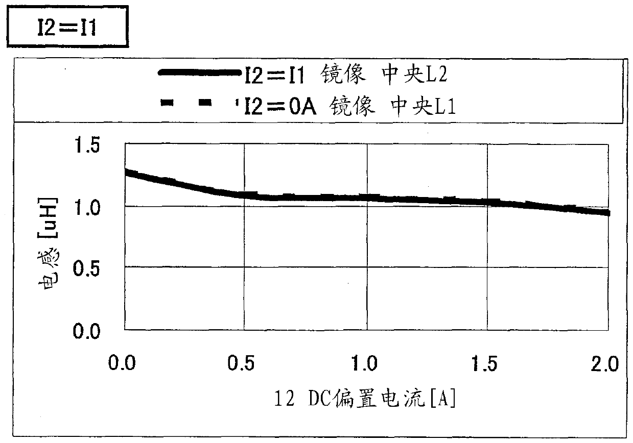
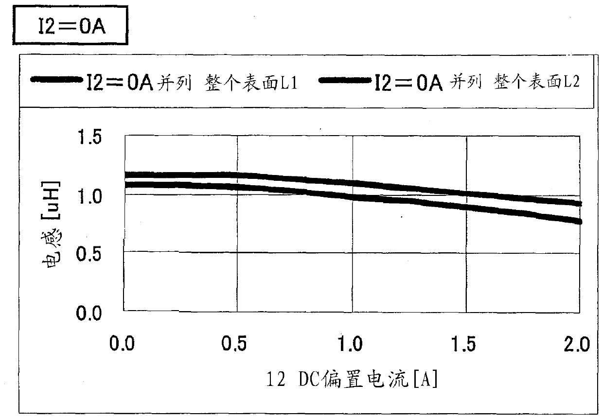
[0051]Then, in the multilayer inductor 1 of the present embodiment, in the magnetic layer 2 , two coils 3 having the same number of windings and the same coil diameter within the manufacturing tolerance range are arranged in parallel so that their axes are parallel to each other. Here, the coils 3 are arranged in a mirror-image relationship...

no. 2 approach )

[0056] Figure 2A , Figure 2B , Figure 2C It is a figure which shows the 2nd Embodiment of the laminated|multilayer inductor of this invention. Again, yes Figure 1A~Figure 1C Parts of the same structure shown are given the same reference numerals and their description is simplified.

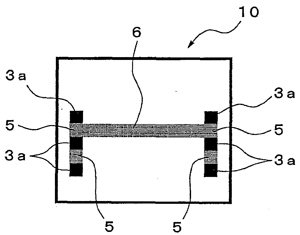
[0057] In the multilayer inductor 10 of the present embodiment, in the first embodiment, the layer of the non-magnetic layer 6 is formed inside the coil 3 , and the non-magnetic layer 6 and the non-magnetic pattern 5 are further formed outside the coil 3 continuously. That is, in place of the magnetic layer 2 described above, an electrically insulating non-magnetic layer 8 is arranged on the entire surface of the outer peripheral portion 7 where the end portion 4 of the coil 3 is arranged.

no. 3 approach )

[0059] Figure 3A , Figure 3B , Figure 3C It is a diagram showing a third embodiment of the present invention. In the multilayer inductor 20, the non-magnetic layer 6 is continuously formed inside the coil 3 between the non-magnetic pattern 5 between the third layer and the conductive pattern 3a, and, Furthermore, the non-magnetic pattern 5 between the seventh layer and the non-magnetic layer 6 inside the coil 3 and the conductive pattern 3 a is continuously electrically insulated outside the coil 3 , that is, the entire surface of the outer peripheral portion 7 of the end portion 4 where the coil 3 is arranged. In place of the above-mentioned magnetic layer 2, a magnetic non-magnetic layer 8 is used.

[0060] According to the laminated inductors 1 , 10 , and 20 having the above structures, the two coils 3 having substantially the same number of windings and coil diameters are arranged in a mirror-image relationship with respect to the virtual planes between the coils 3 . ...


PUM


Abstract

To provide a multilayer inductor capable of reducing the difference in inductance value and suppressing the generation of magnetic interference through a simple operation scheme. According to the present invention, a plurality of electrically insulating magnetic layers 2 and conductive patterns 3a are laminated, and the respective conductive patterns (3a) are sequentially connected in the stacking direction, thereby forming two coils ( 3), the two coils (3) are in a mirror image relationship with respect to the imaginary plane between the two coils (3), and the mutual ends (4) are located on the outer peripheral parts on the opposite side with respect to the above-mentioned imaginary plane Arranged side by side in the manner of stacking, the electrically insulating non-magnetic pattern (5) having the same shape is arranged between the adjacent conductive patterns (3a) in the stacking direction, and only inside the coil (3) is arranged in the stacking direction One or more electrically insulating non-magnetic layers ( 6 ) are provided instead of the magnetic layer ( 2 ).

Description

technical field [0001] The present invention relates to a laminated inductor in which two coils connected to a conductive pattern are arranged in an electrically insulating magnetic layer formed by lamination. Background technique [0002] Generally, a circuit board of a cellular phone or the like is used as a surface-mounted laminated inductor such as a power inductor, and a plurality of coils are arranged inside. [0003] In such a laminated inductor, when the same coils are arranged in parallel, there are problems such as differences in the inductance values ​​due to variations in the magnetic circuit and the positional accuracy of the manufacturing process, and the like. When used as a power inductor, magnetic interference occurs between adjacent coils, and the inductance value of the other inductor changes according to the usage of one inductor. [0004] Therefore, the following Patent Document 1 has conventionally proposed a hybrid electronic component in which a gree...

Claims


Application Information

Patent Timeline
Patent Type & Authority Patents(China)
IPC IPC(8): H01F17/00
CPCH01F17/0013H01F2017/0066H01F27/245H01F27/2804H01F2027/2809
Inventor 松林大介北冈干雄山内清久铃木美那子
Owner NJ COMPONENTS CO LTD
Features
  • R&D
  • Intellectual Property
  • Life Sciences
  • Materials
  • Tech Scout
  • Unparalleled Data Quality
  • Higher Quality Content
  • 60% Fewer Hallucinations
Learn More