Electroplating device for printed circuit board

A technology for printed circuit boards and electroplating devices, which is applied to circuits, electrodes, electrolytic components, etc., can solve the problems of inability to reduce energy consumption, difficult to reduce, and difficult to improve electroplating efficiency, so as to improve electroplating efficiency, reduce output power, and improve The effect of thickness uniformity

Active Publication Date: 2015-11-18
AKM ELECTRONICS TECH SUZHOU
View PDF13 Cites 14 Cited by
  • Summary
  • Abstract
  • Description
  • Claims
  • Application Information

AI Technical Summary

Problems solved by technology

[0003] Just because of the nozzle 3 that is arranged between the anode plate and the printed circuit board, the spacing B between the printed circuit board 1 and the anode plate 2 as the cathode in the existing electroplating device for printed circuit boards (usually the spacing B is both greater than 15cm), it is difficult to shrink, and the width of the upper and lower ends of the printed circuit board 1 after electroplating reaches 1-2cm
Therefore, because the distance B between the cathode and the anode cannot be reduced, the electroplating efficiency of the existing electroplating device for printed circuit boards is difficult to improve, and the energy consumption level cannot be reduced.

Method used


Image

  • Electroplating device for printed circuit board
  • Electroplating device for printed circuit board
  • Electroplating device for printed circuit board

Examples


Embodiment 1

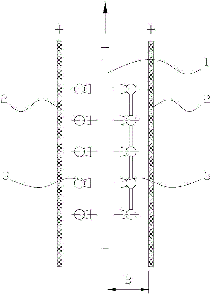
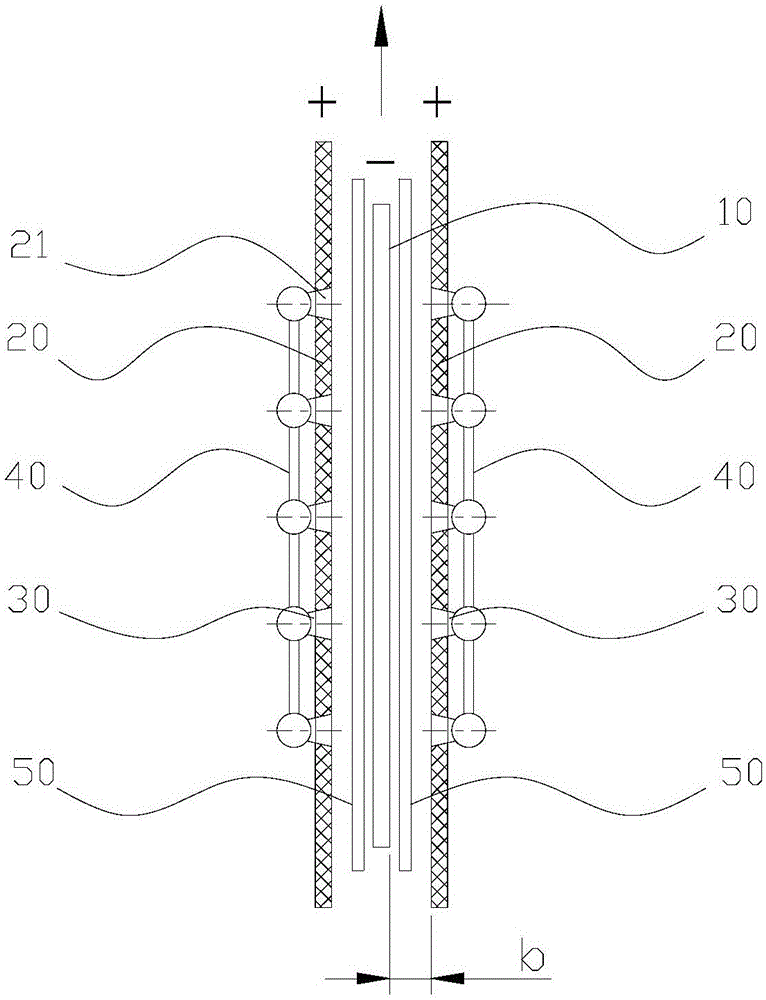
[0025] see figure 2 and 3 , an electroplating device for a printed circuit board, comprising: an electroplating tank for the passage of a printed circuit board 10 in the middle, anode plates 20 arranged on both sides of the printed circuit board 10, arranged in the electroplating tank with the opening facing the printed circuit A plurality of nozzles 30 of the board 10 , nozzles 40 communicating with the plurality of nozzles 30 , insulating baffles 50 arranged on both sides of the printed circuit board 10 , and a vertical lifting device for driving the insulating baffles 50 to reciprocate up and down. When only one side of the printed circuit board 10 is electroplated, an anode plate 20 can be provided only on the outside of the side to be electroplated.

[0026] The anode plate 20 is provided with a through hole 21 penetrating along its thickness direction, the nozzle 30 is fixedly arranged on the anode plate 20 and the opening of the nozzle 30 matches the through hole 21 ....

Embodiment 2

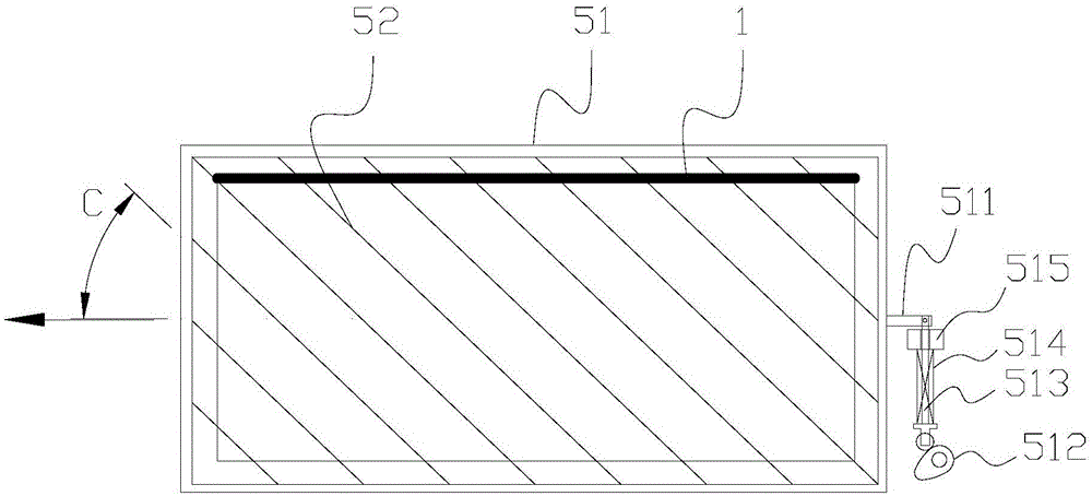
[0033] The structure of this embodiment is basically the same as that of Embodiment 1, the difference is that in the insulating baffle, the plurality of insulated wires are included along the moving direction of the printed circuit board 10 through the electroplating bath (such as Figure 4 The direction indicated by the arrow) the first group of insulated wires 52 arranged in parallel at a first inclination angle, the second group of insulated wires 53 arranged in parallel at a second inclination angle with the moving direction of the printed circuit board 10 passing through the electroplating tank, the second group of insulated wires 53 One group of insulated wires 52 and the second group of insulated wires 53 are arranged to cross each other.


PUM


Abstract

The invention provides an electroplating device for a printed circuit board. The electroplating device comprises a plating tank the middle part of which is used for passing through of the printed circuit board, one or more anode plates arranged at any one side or two sides of the printed circuit board, and nozzles which are arranged in the planting tank and are opened towards the printed circuit board, wherein through holes penetrating through along the thickness direction thereof are formed in the anode plate; the nozzles are fixedly arranged on the anode plate; and the openings of the nozzles are matched with the through holes. Compared with the prior art, on the premise of not changing the distance between the nozzles and the printed circuit board, the distance between the printed circuit board serving as a cathode and the anode plate is greatly shortened to 2-3cm, on the one hand, the thickness uniformity of a surface electroplated coating of the printed circuit board is effectively improved, and on the other hand, the electroplating efficiency is greatly enhanced, and the energy consumption is lowered.

Description

technical field [0001] The invention relates to an electroplating device for a printed circuit board. Background technique [0002] Electroplating is a very important process in the manufacturing process of printed circuit boards (PCB, Printed Circuit Board). It uses electrolysis to grow metal layers in the wires and through holes of printed circuit boards, thereby protecting exposed copper printed lines and connection holes. . At present, the electroplating of printed circuit boards mainly adopts continuous automatic electroplating equipment, such as figure 1 As shown, the printed circuit board 1 serving as the cathode is continuously moved through the electroplating tank, and anode plates 2 are respectively arranged on both sides of the printed circuit board 1 in the electroplating tank. A plurality of nozzles 3 are also arranged between the anode plate 2 and the printed circuit board 1, and the electroplating solution is sprayed from the nozzles 3 and sprayed vertically...

Claims


Application Information

Patent Timeline
Patent Type & Authority Applications(China)
IPC IPC(8): C25D7/12C25D5/08
CPCC25D5/08C25D17/00C25D17/12
Inventor 王靖王锋伟
Owner AKM ELECTRONICS TECH SUZHOU
Why Eureka
Try Eureka