Processing method of multi-signal board level clock domain crossing

A processing method and clock domain technology, applied in the technical improvement field of cross-board clock domain, can solve problems such as non-appearance, system impact, unsatisfied data establishment and guaranteed time, etc.

Inactive Publication Date: 2015-11-18
安徽华明航空电子系统有限公司
View PDF6 Cites 2 Cited by
  • Summary
  • Abstract
  • Description
  • Claims
  • Application Information

AI Technical Summary

Problems solved by technology

But this method has limitations, you can only hope that the glitch does not appear on the clock edge, or the establishment and guarantee time of the data a

Method used


Image

  • Processing method of multi-signal board level clock domain crossing
  • Processing method of multi-signal board level clock domain crossing
  • Processing method of multi-signal board level clock domain crossing

Examples


Embodiment Construction

[0018] The invention aims at the shortcomings and deficiencies of the general methods for eliminating the effects of burrs, and provides a method for eliminating the effects of burrs with wider applicable range and stricter restrictions than the traditional method. The invention is suitable for eliminating the influence of burrs in the FPGA design not exceeding 100MHZ.

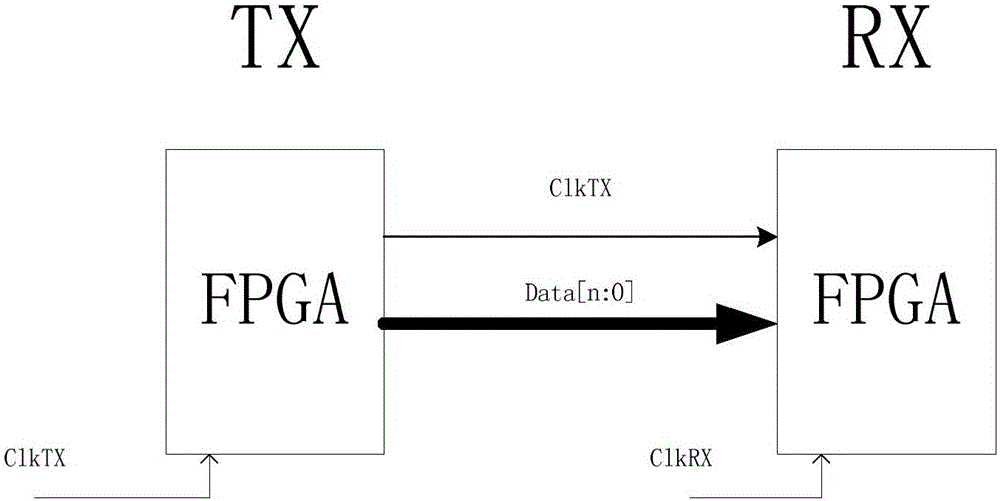
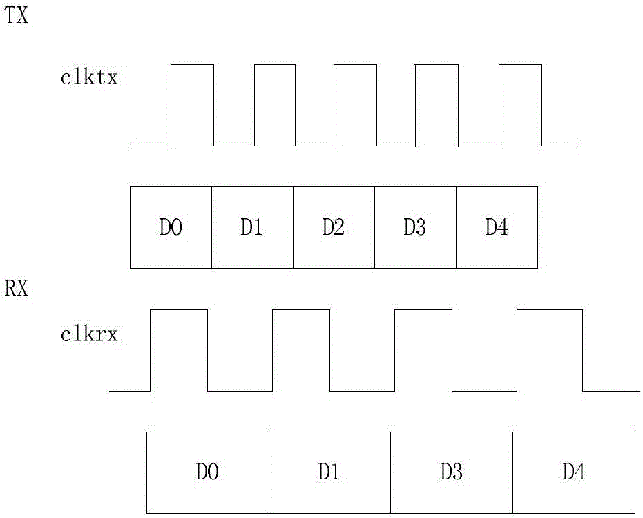
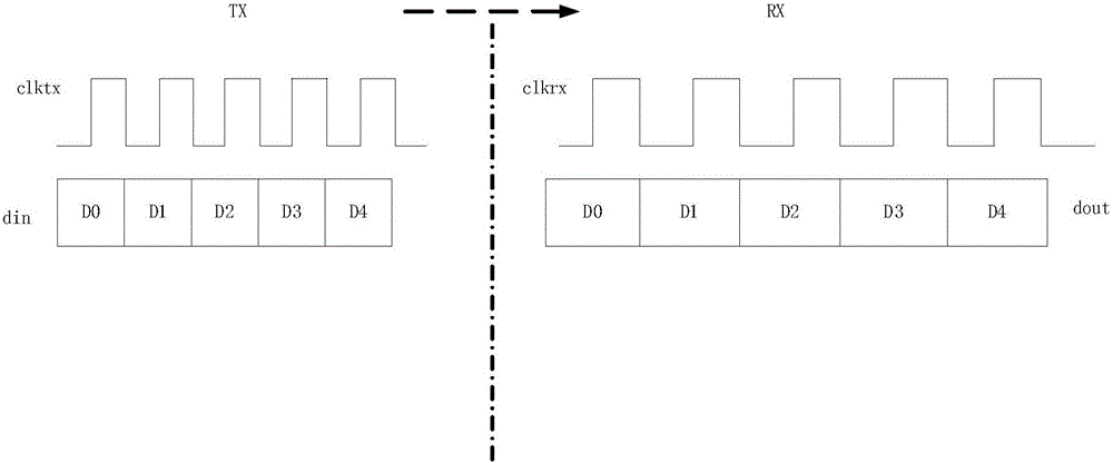
[0019] figure 1 TX is the transmitting domain, the clock reference is ClkTX, RX is the receiving domain, and the clock reference is ClkRX. ClkTX and Data[n:0] in the transmitting domain are sent to the receiving domain through the cable. The receiving domain must ensure that the received data is correct data before processing the data. In FPGA, data is usually sent and received on the rising or falling edge of the clock. Assume that the sending domain clock is clktx and the receiving domain clock is clkrx. Clktx and clkrx cannot be exactly the same clock. When receiving data at the receiving end, the data ...


PUM


Abstract

The invention discloses a processing method of multi-signal board level clock domain crossing. The method is characterized by comprising the following steps: arranging a memory between a transmission domain TX and a reception domain RX, writing data into the memory by the transmission domain TX under a clktx clock and reading the data out of the memory by the reception domain RX under the clkrx clock; connecting the reception domain RX to a burr processing module which is used for detecting high level of the clock; considering the clock as an active clock when the high level achieves a certain length; and considering the clock as burr when a high level signal with a certain width is output and lowering the level. By adopting the method, the influences caused by the burrs during the clock domain crossing are eliminated while the synchronization of asymmetric signals is completed, excessive production cost is not required and the method is simple and convenient.

Description

technical field [0001] The invention relates to the technical improvement of cross-board clock domains, in particular to a processing method for multi-signal cross-board clock domains. Background technique [0002] In modern electronic design, only the most elementary logic circuits use a single clock, and most designs related to data transmission face a challenge, that is, data transmission across multiple clock domains. The signal is transmitted from one clock domain to another. For the new clock domain, the signal is an asynchronous signal. The asynchronous signal must be synchronized to the new clock domain before subsequent processing can be performed on the synchronized signal. In the test circuit, the clock transmitting domain and the clock receiving domain are usually connected by a cable. This crossing of clock domains is called a cross-board clock domain. [0003] The signal needs to be delayed during transmission, and the delay is related to the length of the co...

Claims


Application Information

Patent Timeline
IPC IPC(8): G11C7/10G11C7/22
Inventor 邴志光孙义军方小伟
Owner 安徽华明航空电子系统有限公司
Why Eureka
Try Eureka