Thin film transistor array substrate, manufacturing method thereof and display device

A technology of thin-film transistors and array substrates, which is applied in the display field and can solve problems such as uneven images, electric leakage, and uneven bending

Active Publication Date: 2015-11-18
BOE TECH GRP CO LTD +1
View PDF5 Cites 6 Cited by
  • Summary
  • Abstract
  • Description
  • Claims
  • Application Information

AI Technical Summary

Problems solved by technology

After analysis, the mechanism of failure is: it is related to the residual sand on the plate electrode layer (such as the common electrode), such as Figure 1a and Figure 1b As shown, the area with severe residual sand is likely to cause the active layer 01 in the thin film transistor to be bent and uneven, resulting in a large Ioff characteristic of the thin film transistor, serious leakage, and uneven picture

Method used


Image

  • Thin film transistor array substrate, manufacturing method thereof and display device
  • Thin film transistor array substrate, manufacturing method thereof and display device
  • Thin film transistor array substrate, manufacturing method thereof and display device

Examples


Embodiment Construction

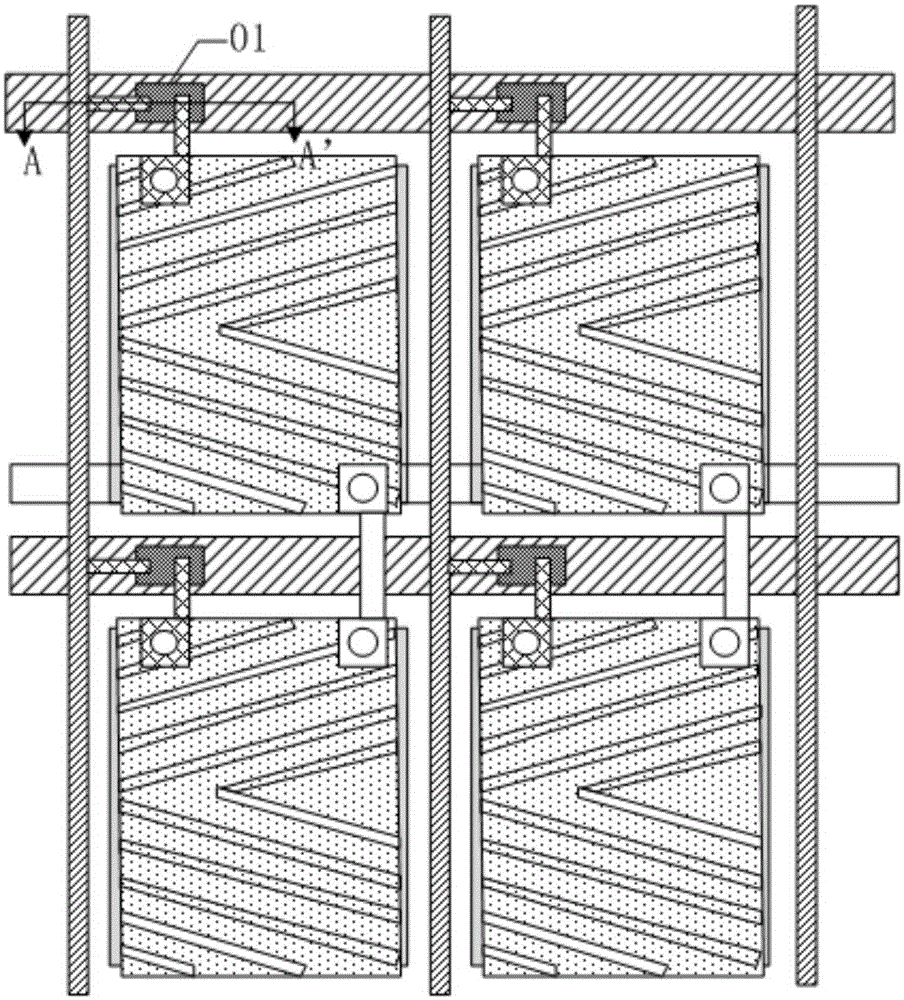
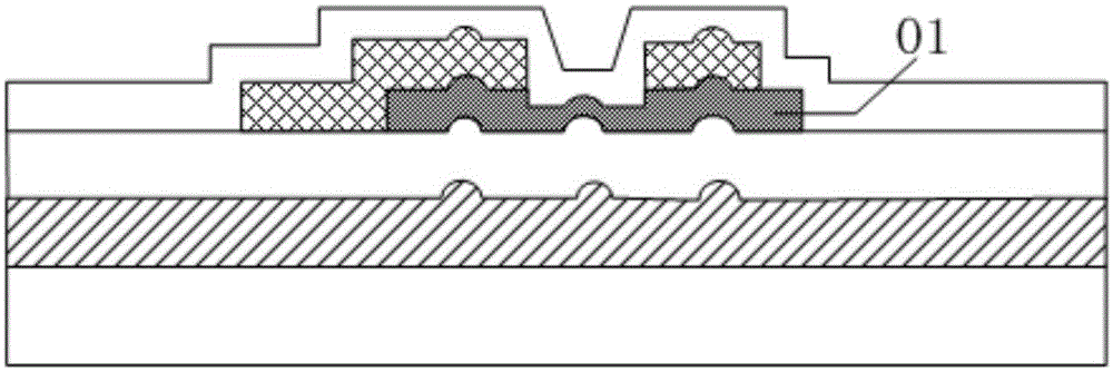
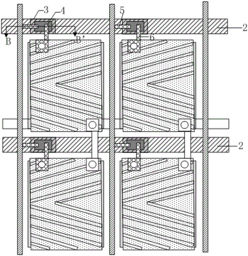
[0040] The specific implementations of the thin film transistor array substrate provided by the embodiments of the present invention, its manufacturing method and the display device will be described in detail below with reference to the accompanying drawings.

[0041] Wherein, the thickness and shape of each film layer in the drawings do not reflect the real ratio of the thin film transistor array substrate, and the purpose is only to illustrate the content of the present invention.

[0042] An embodiment of the present invention provides a thin film transistor array substrate, such as Figure 2a to Figure 2c As shown, it includes: a base substrate 1, a gate disposed on the base substrate 1, and a gate insulating layer and an active layer 4 sequentially disposed on the gate;

[0043] Also includes: a pixel electrode, a common electrode and a transparent electrode layer 3 arranged on the base substrate 1; wherein,

[0044] The transparent electrode layer 3 is the same layer a...


PUM


Abstract

The invention discloses a thin film transistor array substrate, a manufacturing method thereof and a display device. The thin film transistor array substrate comprises a substrate, a grid arranged on the substrate, a grid insulating layer and an active layer sequentially arranged on the grid, and a pixel electrode, a public electrode and a transparent electrode layer which are arranged on the substrate, wherein the transparent electrode layer and the pixel electrode / public electrode are arranged on the same layer and made of same materials; the transparent electrode layer is arranged under the grid insulating layer; and forward projection of the active layer on the substrate is positioned in a region where forward projection of the transparent electrode layer is arranged. Since the transparent electrode layer which is arranged at the same layer of the pixel electrode / public electrode and has the same material of the pixel electrode / public electrode is arranged just under the active layer in a thin film transistor, the electrode layer residual sand of the region where the thin film transistor is positioned can be reduced, so that the surface of the active layer is smooth, the phenomenon of uneven image caused by residual sand is avoided, the implementation method is simple, the influence on grid resistance is small, and the product quality can be improved.

Description

technical field [0001] The invention relates to the field of display technology, in particular to a thin film transistor array substrate, a manufacturing method thereof and a display device. Background technique [0002] At present, the Advanced Super Dimension Switch (ADS for short) thin film transistor liquid crystal display uses the electric field generated by the edge of the slit electrode in the same plane and the multi-dimensional electric field formed between the slit electrode layer and the plate electrode layer to make the inside of the liquid crystal cell All oriented liquid crystal molecules between the slit electrodes and directly above the electrodes can be rotated, thereby improving the working efficiency of the liquid crystal and increasing the light transmittance. Therefore, ADS technology can improve the picture quality of the product, and has the advantages of high resolution, high transmittance, low power consumption, and wide viewing angle. [0003] The ...

Claims


Application Information

Patent Timeline
IPC IPC(8): H01L27/12H01L21/77H01L21/768G02F1/1343
CPCH01L21/768H01L29/42384H01L29/4908H01L29/78603H01L27/1218G02F1/1362H01L27/124H01L27/127G02F1/13629G02F1/136295G02F1/1343G02F1/134309G02F1/13439G02F1/136286G02F1/1368G02F2201/121G02F2201/123
Inventor 冯伟
Owner BOE TECH GRP CO LTD
Why Eureka
Try Eureka