Pixel structure and manufacture method thereof

A technology of pixel structure and manufacturing method, which is applied in semiconductor/solid-state device manufacturing, electrical components, electric solid-state devices, etc., and can solve problems such as inconsistent luminous efficiency of sub-pixels of different colors, low blue light efficiency of organic light-emitting diode displays, etc.

Inactive Publication Date: 2015-11-18
AU OPTRONICS CORP
View PDF4 Cites 28 Cited by
  • Summary
  • Abstract
  • Description
  • Claims
  • Application Information

AI Technical Summary

Problems solved by technology

[0006] The problem to be solved by the present invention is the low blue light efficiency of organic light-emitting diode displays and the inconsistent luminous efficiency of sub-pixels of different colors after the miniaturization of inorganic light-emitting diodes.

Method used


Image

  • Pixel structure and manufacture method thereof
  • Pixel structure and manufacture method thereof

Examples


Embodiment Construction

[0048] A number of implementations of the present invention will be disclosed below with the accompanying drawings. For the sake of clarity, many practical details will be described together in the following description. It should be understood, however, that these practical details should not be used to limit the invention. That is, in some embodiments of the present invention, these practical details are unnecessary. In addition, for the sake of simplifying the drawings, some existing conventional structures and elements will be shown in a simple and schematic way in the drawings.

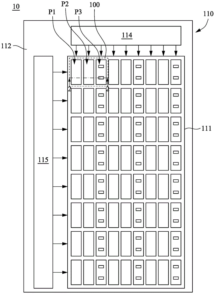
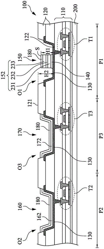
[0049] Please refer to figure 1 and figure 2 , figure 1 It is a top view of a light-emitting display device 10 according to an embodiment of the present invention, figure 2 for along figure 1 Sectional view of line segment 2-2. As shown in the figure, the light emitting display device 10 includes a substrate 200 . The substrate 200 may include a pixel area 111 and a non-pixel area 112 . ...


PUM


Abstract

The invention provides a pixel structure and manufacture method thereof. The pixel structure comprises a substrate and pixel units on the substrate. Each of the pixel unit comprises a pixel circuit structural layer, a pixel definition layer, a pixel electrode, inorganic LED subpixel and a first OLED subpixel. The pixle circuit structural layer is formed on the surface of the substrate; the pixel definition layer is formed on the pixel circuit structural layer and has a first opening and a second opening; the pixel electrode is disposed in the first and second openings and electrically connected with the pixle circuit structural layer; the inorganic LED subpixel comprises an ahesion layer, a first semiconductor layer, a second semiconductor layer; the first OLED subpixel comprises a first transmission layer and a second transmission layer; beam emitted by the inorganic LED subpixel has a different color from that of beam emitted by the first OLED subpixel. The pixel structure can solve problems that blue light OLED subpixel has a relatively low luminous efficiency, and that red light OLED has a relatively low luminous efficiency after miniaturation.

Description

technical field [0001] The present invention relates to the field of display technology, in particular to a pixel structure and a manufacturing method thereof. Background technique [0002] With the advancement of technology, the display has gradually changed from a relatively thick cathode ray tube (Cathode Ray Tube, CRT) display to a relatively flat and thin liquid crystal display (Liquid Crystal Display, LCD) or organic light emitting diode (Organic Light Emitting Diode, OLED) display. [0003] The liquid crystal display uses the backlight module to emit light, and generates light of different brightness and color through liquid crystal molecules and color filters respectively. Therefore, each pixel of the liquid crystal display cannot emit light by itself, and it is a passive light-emitting display. LCD monitors have a long lifespan and do not suffer from image burn-in. In addition, with the development of thin film transistor technology, each pixel in the liquid cryst...

Claims


Application Information

Patent Timeline
Patent Type & Authority Applications(China)
IPC IPC(8): H01L27/32H01L21/70
Inventor 萧翔允刘康弘刘品妙吴宗典陈振彰张正杰林宗毅
Owner AU OPTRONICS CORP
Why Eureka
Try Eureka