A display device and pixel circuit thereof

A technology of pixel circuit and voltage source, applied in static indicators, instruments, etc., can solve problems such as uneven display

Active Publication Date: 2017-11-28
PEKING UNIV SHENZHEN GRADUATE SCHOOL
View PDF8 Cites 0 Cited by
  • Summary
  • Abstract
  • Description
  • Claims
  • Application Information

AI Technical Summary

Problems solved by technology

[0006] The present application provides a display device and its pixel circuit, which can compensate the threshold voltage shift of the driving transistor and the light-emitting device, and can also solve the problem of uneven display caused by the different threshold voltages of the driving transistors in various parts of the display panel.

Method used


Image

  • A display device and pixel circuit thereof
  • A display device and pixel circuit thereof
  • A display device and pixel circuit thereof

Examples


Embodiment 1

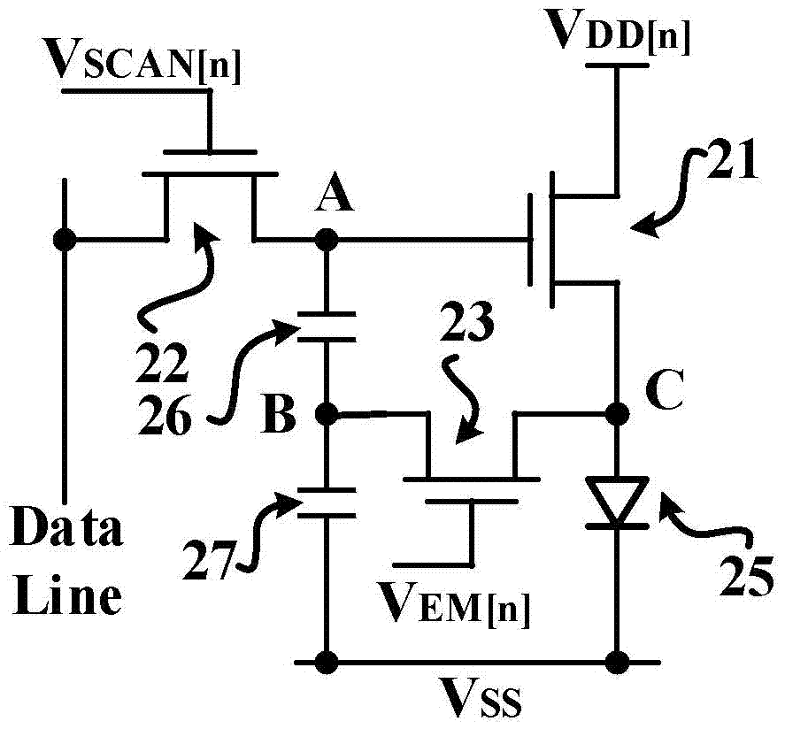
[0073] Please refer to figure 2 , this embodiment provides a pixel circuit, including a first transistor 21, a second transistor 22, a third transistor 23, a first capacitor 26, a second capacitor 27 and a light emitting device 25,

[0074] The first transistor 21 and the light emitting device 25 are serially connected to the first voltage source signal terminal V DD[n] and the second voltage source signal terminal V SS between. The control pole of the first transistor 21 is connected to the second pole of the second transistor 22, the first pole of the first transistor 21 is connected to the first voltage source signal terminal, and the second pole of the first transistor 21 is connected to the anode of the light emitting device 25 ;

[0075] The control electrode of the second transistor 22 is connected to the first scanning control signal terminal V SCAN[n] , used to receive the first scan control signal of the current row, the first pole of the second transistor 22 is...

Embodiment 2

[0096] Such as Figure 4 As shown, this embodiment provides another pixel circuit, and its main difference from Embodiment 1 is that a fourth transistor 24 is added, and the fourth transistor 24 controls the second pixel circuit in the circuit under the control of the third scanning signal. Node B and the third node C are initialized; at this time, the first voltage source signal terminal V DD The input is no longer a pulse signal, but a constant high level, and the initialization is completed by the fourth transistor 24 .

[0097] The control electrode of the fourth transistor 24 is connected to the third scanning control signal terminal V R[n] , the first pole is connected to the anode of the light emitting device 25, and the second pole is connected to the third voltage source signal terminal V CM , for responding to the third scan control signal, to initialize the voltages of the second node B and the third node C to a certain low level in the initialization phase.

[0...

Embodiment 3

[0102] Please refer to Figure 6 , this embodiment provides another pixel circuit, its main difference from Embodiment 2 is that a fifth transistor 28 is added, and the control electrode of the fifth transistor 28 is connected to the fourth scanning signal terminal V SN[n] , the first pole is connected to the fourth voltage source signal terminal for inputting a constant reference voltage V REF , the second electrode is connected to the control electrode of the first transistor 21 . Under the control of the fourth scanning signal, the fifth transistor 28 provides a constant reference voltage V REF The benefit of doing this is that the row programming time can be greatly reduced, making the pixel circuit more suitable for large-area, high-resolution, high-frame-rate displays.

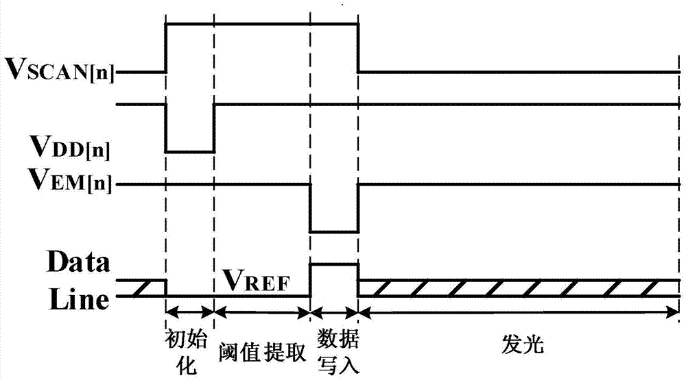
[0103] The driving signal waveform diagram of the pixel circuit in this embodiment is as follows Figure 7 As shown, a frame time T is also divided into four phases: an initialization phase, a thresho...


PUM


Abstract

A display device and its pixel circuit. The pixel circuit generates the threshold voltage information of the driving tube in the form of source follower, and generates the threshold voltage and the gray value of the driving tube at both ends of the first capacitor through the voltage division of the first capacitor and the second capacitor. During the light-emitting process, the reference voltage remains unchanged, so that the driving current flowing through the light-emitting device has nothing to do with the threshold voltage of the driving transistor and the light-emitting device, thereby compensating for the threshold voltage shift of the driving transistor and the light-emitting device. Solve the problem of uneven display on the display panel. When the display device adopts the row-by-row lighting method, it adopts the form of overlapping scanning control signals to reduce the row programming time of the circuit, and meet the requirements of high-resolution and high frame rate display panels while obtaining high precision; when using the concentrated lighting method , The pixel circuit adopts group programming and group lighting to reduce circuit complexity and increase lighting time.

Description

technical field [0001] The present application relates to the field of display technology, in particular to a display device and a pixel circuit thereof. Background technique [0002] Organic light-emitting diode (OLED, Organic Light-Emitting Diode) display has been widely studied in recent years due to its advantages of high brightness, high luminous efficiency, wide viewing angle, low power consumption, and low manufacturing cost, and has been rapidly applied to a new generation of displays. device. OLED displays can be divided into two types: PMOLED (Passive Matrix OLED, passive matrix OLED) and AMOLED (Active Matrix OLED, active matrix OLED) according to the pixel driving method. Although PMOLED has low manufacturing cost, it has crosstalk and requires a large driving current, so it has disadvantages such as short service life and high power consumption, and cannot meet the display requirements of large area and high resolution. In contrast, AMOLED avoids problems such...

Claims


Application Information

Patent Timeline
Patent Type & Authority Patents(China)
IPC IPC(8): G09G3/3233
CPCG09G3/3233G09G2300/0819G09G2300/0852G09G2300/0861G09G2310/0216G09G2310/0218G09G2320/0233G09G2320/045G09G3/2018G09G3/3266G09G3/3291G09G2300/0426G09G2310/0289G09G2310/08G09G2320/064
Inventor 张盛东王翠翠冷传利
Owner PEKING UNIV SHENZHEN GRADUATE SCHOOL
Why Eureka
Try Eureka