Semiconductor device and method of forming the same

A semiconductor and device technology, applied in the field of semiconductor devices and their formation, can solve problems such as difficulty in adjusting the threshold voltage of semiconductor devices, and achieve the effects of excellent electrical performance, reduced process difficulty, and good performance

Active Publication Date: 2018-03-30
SEMICON MFG INT (SHANGHAI) CORP
View PDF3 Cites 0 Cited by
  • Summary
  • Abstract
  • Description
  • Claims
  • Application Information

AI Technical Summary

Problems solved by technology

[0006] The problem solved by the present invention is to provide a semiconductor device and its forming method, solve the problem that it is difficult to adjust the threshold voltage of the semiconductor device, and at the same time ensure that the probability of soft errors in the semiconductor device is low

Method used


Image

  • Semiconductor device and method of forming the same
  • Semiconductor device and method of forming the same
  • Semiconductor device and method of forming the same

Examples


Embodiment Construction

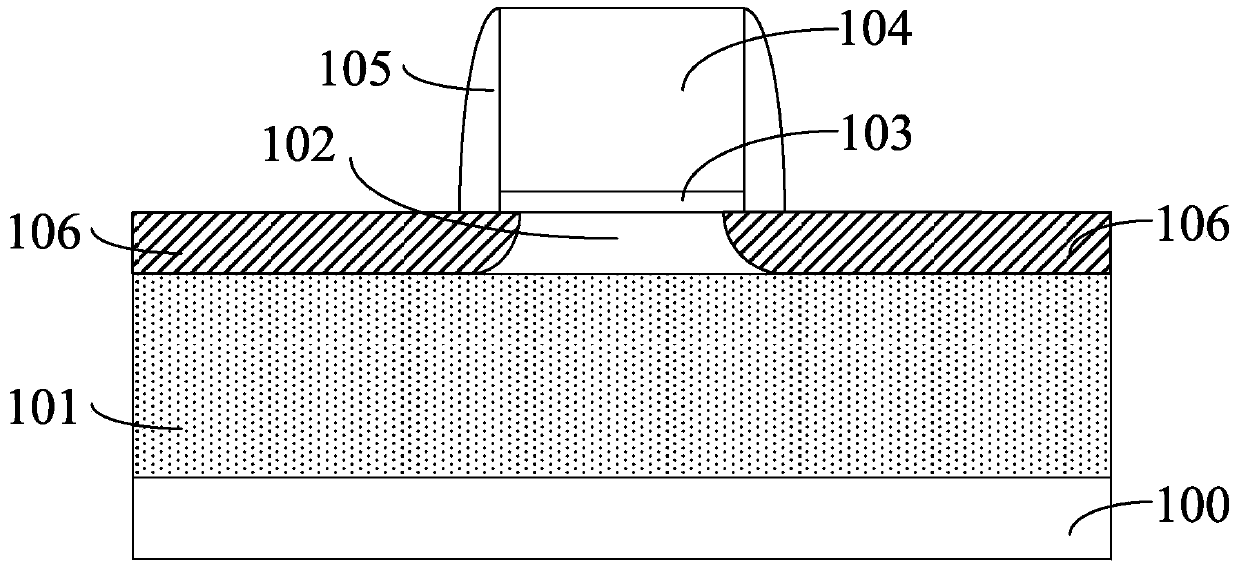
[0026] It can be seen from the background art that the threshold voltage of the semiconductor device in the prior art is difficult to adjust, and the application of the semiconductor device is limited.

[0027]According to the research on semiconductor devices, it is found that the threshold voltage of semiconductor devices manufactured on SOI substrates is substantially achieved by changing the bias voltage on the bottom silicon layer. Usually by applying a body bias voltage (body bias voltage) to the bottom silicon layer, the voltage value on the top silicon layer (that is, the channel region) under the gate structure is changed in order to adjust the threshold voltage of the semiconductor device; however, although When a large bias voltage is applied to the bottom silicon layer, the improvement of the threshold voltage of the semiconductor device is limited.

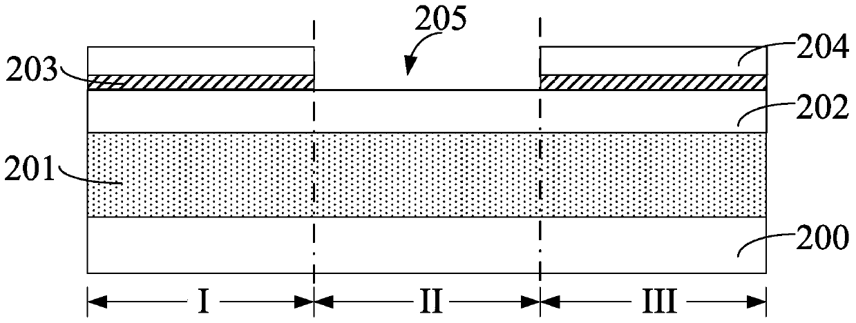
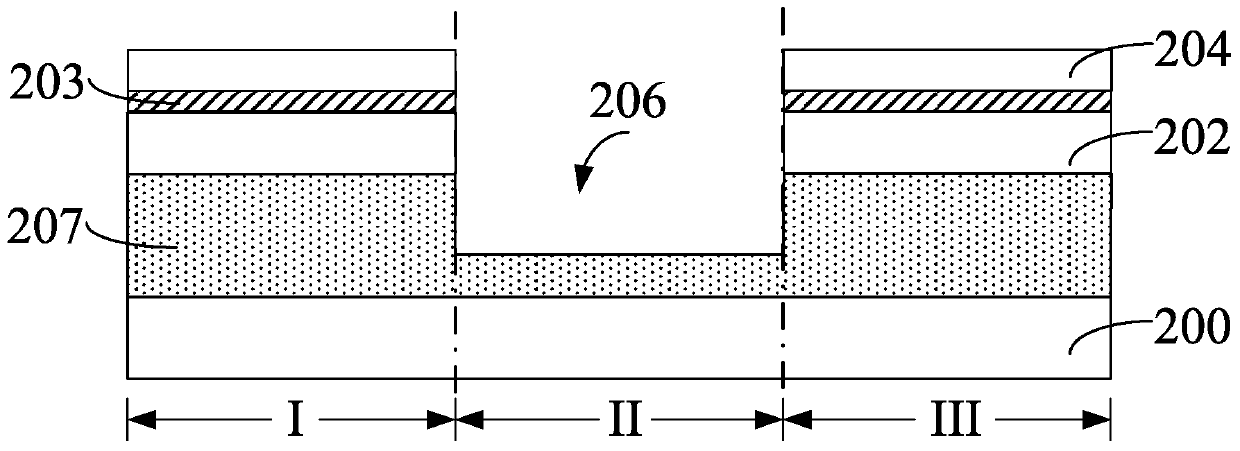
[0028] Further research on semiconductor devices has found that after applying a bias voltage to the bottom silicon...


PUM


Abstract

A semiconductor device and a method for forming the same, wherein the method for forming the semiconductor device includes: providing a substrate, the substrate including a first semiconductor layer, an insulating layer positioned on the surface of the first semiconductor layer, and a second semiconductor layer positioned on the surface of the insulating layer, The substrate has a first region, a second region and a third region, the second region is adjacent to the first region and the third region, wherein the thickness of the insulating layer in the first region and the third region is greater than that of the insulating layer in the second region The bottom surface of the insulating layer in the first region, the second region and the third region is flush; the gate structure is formed on the surface of the second semiconductor layer in the second region; the first region and the third region on both sides of the gate structure A doped region is formed in the second semiconductor layer. The thickness of the insulating layer under the gate structure of the present invention is smaller than the thickness of the insulating layer under the doped region. Since the effective resistance of the insulating layer under the gate structure is small, the threshold voltage of the semiconductor device can be effectively improved.

Description

technical field [0001] The invention relates to the technology in the field of semiconductor manufacturing, in particular to a semiconductor device and a forming method thereof. Background technique [0002] With the advancement of semiconductor technology, integrated circuits are developing towards high integration, high speed and low power consumption. The process of bulk silicon (Bulk Silicon) substrates and bulk silicon devices (devices manufactured based on bulk silicon substrates) is approaching Physical limits, severe challenges are encountered in further reducing the feature size of integrated circuits. At present, the industry believes that silicon-on-insulator (SOI: Silicon on Insulator) substrates and SOI devices are one of the best solutions to replace bulk silicon and bulk silicon devices. [0003] SOI substrate is a kind of substrate used in the manufacture of integrated circuits. Compared with bulk silicon substrates currently widely used, SOI substrates have...

Claims


Application Information

Patent Timeline
Patent Type & Authority Patents(China)
IPC IPC(8): H01L21/84H01L27/12
Inventor 刘金华
Owner SEMICON MFG INT (SHANGHAI) CORP
Why Eureka
Try Eureka