Manufacturing method of printed circuit board ink plug hole

A technology for printed circuit boards and manufacturing methods, which is applied in the secondary processing of printed circuits, the formation of electrical connections of printed components, and the application of non-metallic protective layers. It can solve the problems of ink spillage and oil explosion in holes, and prevent explosions The effect of oil problems

Active Publication Date: 2015-11-25
SHENZHEN SUNTAK MULTILAYER PCB
View PDF4 Cites 17 Cited by
  • Summary
  • Abstract
  • Description
  • Claims
  • Application Information

AI Technical Summary

Problems solved by technology

[0004] The purpose of the present invention is to provide a method for making ink plug holes in printed circuit boards, aiming at solving the problem of ink overf

Method used


Image

  • Manufacturing method of printed circuit board ink plug hole
  • Manufacturing method of printed circuit board ink plug hole
  • Manufacturing method of printed circuit board ink plug hole

Examples


Embodiment Construction

[0029] In order to make the object, technical solution and advantages of the present invention clearer, the present invention will be further described in detail below in conjunction with the accompanying drawings and embodiments. It should be understood that the specific embodiments described here are only used to explain the present invention, not to limit the present invention.

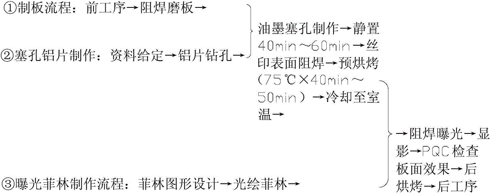
[0030] Please refer to Figure 3 to Figure 9 , the manufacturing method of the printed circuit board ink plug hole provided by the embodiment of the present invention comprises the following steps:

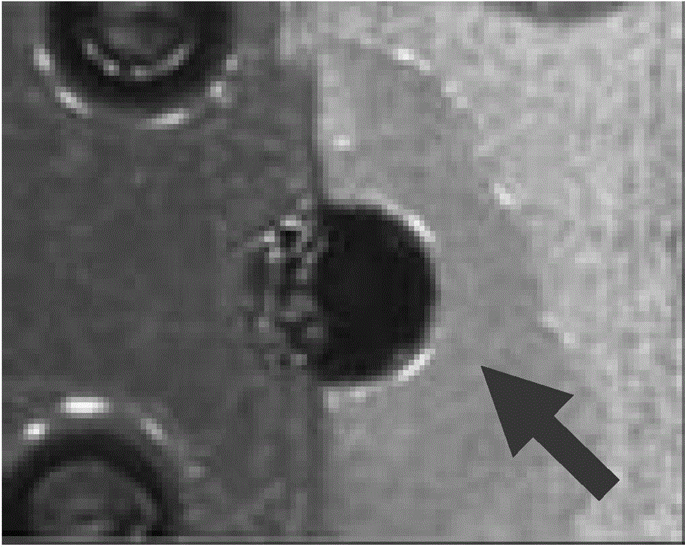
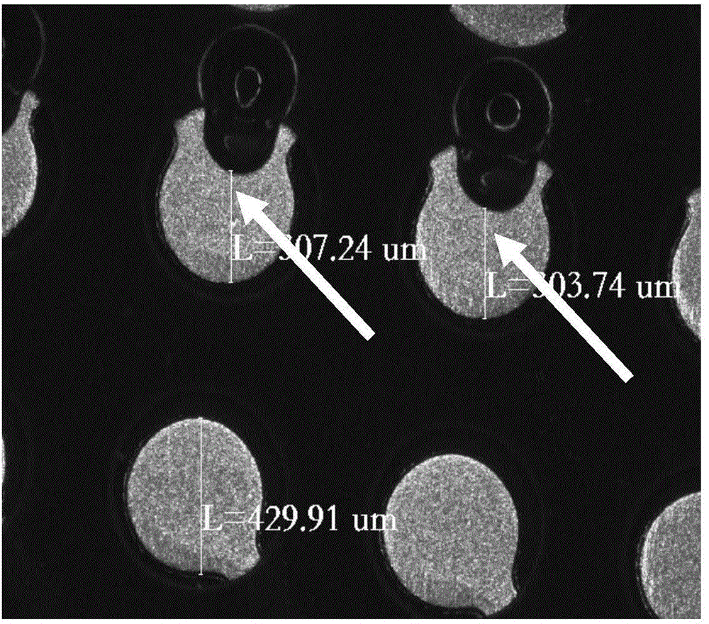
[0031] S1: Provide a circuit board, the circuit board is provided with an oil plug hole 10, and the oil plug hole 10 penetrates the circuit board along the stacking direction of the circuit board; understandably, the memory copper thickness of the circuit board Not less than 2 ounces (OZ), preferably, in this step, also include the step of grinding plate, through grinding plate step, make described ci...


PUM


Abstract

The invention is suitable for the technical field of printed circuit board processing, provides a manufacturing method of a printed circuit board ink plug hole, and aims to solve the problem that ink in a hole easily spills over in a manufacturing method of a printed circuit board ink plug hole in the prior art and the problem that an oil explosion phenomenon occurs in a baking process. The manufacturing method of the printed circuit board ink plug hole comprises the following steps: providing a circuit board, fabricating a plug hole aluminum sheet, fabricating an explosive film, performing ink hole plugging, performing resistance welding on a silkscreen surface, performing resistance welding exposure and development, and performing after baking which is performed on the circuit board through adoption of a segmented heating baking mode. By utilizing the segmented heating baking mode, plug hole ink is guaranteed to be cured rhythmically, and the oil explosion problem generated by rapid expansion, caused by one-time high-temperature baking, of the plug hole ink in the oil plug hole is prevented.

Description

technical field [0001] The invention belongs to the technical field of printed circuit board processing, and in particular relates to a method for manufacturing an ink plug hole of a printed circuit board. Background technique [0002] Because some printed circuit boards have special requirements for impedance and post-process manipulator adsorption, etc., it is necessary to carry out the process of making solder resist ink plug holes. At present, the production of solder resist ink plug holes generally uses aluminum sheet plug holes, that is, use an aluminum sheet to drill holes with corresponding apertures at the corresponding positions where ink plug holes are required on the printed circuit board, and stick the aluminum sheet to the mesh. On the frame, form a plug hole aluminum mesh panel. The production process of ink plug orifice plate is as follows: Figure 10 shown. [0003] However, for printed circuit boards with an inner layer copper thickness ≥ 2OZ, after the...

Claims


Application Information

Patent Timeline
IPC IPC(8): H05K3/28H05K3/40
Inventor 朱拓宋建远刘剑锋姜翠红
Owner SHENZHEN SUNTAK MULTILAYER PCB
Why Eureka
Try Eureka