Manufacture method of touch screen and touch screen

A production method and touch screen technology, applied in the input/output process of data processing, instruments, electrical digital data processing, etc., can solve the problems of poor yield rate of GFF architecture, poor price controllability, broken ITO lines, etc. Achieve the effect of reducing the thickness of the whole machine, lowering the cost and increasing the production capacity

Active Publication Date: 2015-12-02
TRULY OPTO ELECTRONICS
View PDF3 Cites 13 Cited by
  • Summary
  • Abstract
  • Description
  • Claims
  • Application Information

AI Technical Summary

Problems solved by technology

However, the GFF architecture has a poor yield rate in large-scale applications. During the manufacturing process, especially during the bonding process, the ITO line is prone to breakage; it contains two layers of Film and two layers of OCA at the same time, making it difficult to reduce the thickness; Scarcity of resources, price controllability is not strong
Although the GFF structure touch screen can still retain the touch function after being broken, it is relatively thick, has low light transmittance, and the production process is relatively cumbersome, which is not conducive to reducing labor and material costs, and the power consumption is high when used in portable electronic products. Light and thin is the main trend of touch screen development

Method used


Image

  • Manufacture method of touch screen and touch screen
  • Manufacture method of touch screen and touch screen
  • Manufacture method of touch screen and touch screen

Examples


Embodiment 1

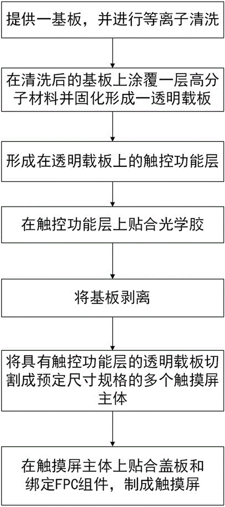
[0062] Such as Figure 4 Shown, a kind of manufacturing method of touch screen specifically comprises the following steps:

[0063] (1) Provide a substrate and perform plasma cleaning;

[0064] (2) Coat a layer of polyimide on the cleaned substrate and cure to form a transparent carrier with a thickness of about 1 μm;

[0065] (3) A layer of ITO film is sputtered on the transparent carrier; the required ITO functional pattern is etched on the ITO film according to the preset functional pattern, and a thickness of about 0.01 μm is directly formed on the transparent carrier. ITO functional pattern layer; during specific implementation, a layer of insulating layer can also be coated on the ITO functional pattern layer;

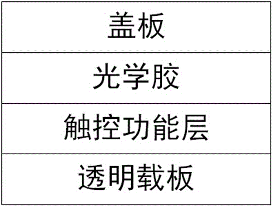
[0066] (4) Paste an OCA optical adhesive with a thickness of about 10 μm on the ITO functional pattern layer prepared in step (3); the optical adhesive has been hollowed out in advance for binding positions;

[0067] (5) Peel off the substrate, and coat a PE p...

Embodiment 2

[0077] Such as Figure 6 Shown, a kind of manufacturing method of above-mentioned touch screen specifically comprises the following steps:

[0078] (1) Provide a substrate and perform plasma cleaning;

[0079] (2) Coat a layer of polyimide on the cleaned substrate and cure to form a transparent carrier with a thickness of about 25 μm;

[0080] (3) A touch function layer with a thickness of about 20 μm formed above the transparent carrier; it specifically includes the following steps:

[0081] A layer of ITO film is sputtered on the transparent carrier, and etched into an ITO bridge;

[0082] Silk-screen insulating oil on the ITO bridge and solidify to form an insulating layer;

[0083] A layer of ITO film is sputtered on the insulating layer, and the required ITO functional pattern is etched on the ITO film according to the preset functional pattern to obtain the ITO functional pattern layer;

[0084] Silk-screen photosensitive silver paste on the ITO functional pattern la...

Embodiment 3

[0097] Such as Figure 8 Shown, a kind of manufacturing method of touch screen specifically comprises the following steps:

[0098] (1) Provide a substrate and perform plasma cleaning;

[0099] (2) Coat a layer of polyimide on the cleaned substrate and cure to form a transparent carrier with a thickness of about 100 μm;

[0100] (3) A touch function layer with a thickness of about 5 μm formed above the transparent carrier; it specifically includes the following steps:

[0101] A layer of ITO film is sputtered on the transparent carrier; the required ITO functional pattern is etched on the ITO film according to the preset functional pattern, and an ITO functional pattern layer directly formed on the transparent carrier is obtained;

[0102] Apply OC insulating glue on the ITO functional pattern layer and cure to form an insulating layer;

[0103] Silver paste is screen-printed on the insulating layer and solidified to obtain a conductive pattern layer;

[0104] (4) Lay an O...


PUM

PropertyMeasurementUnit
thicknessaaaaaaaaaa
thicknessaaaaaaaaaa
thicknessaaaaaaaaaa

Abstract

The invention discloses a manufacture method of a touch screen and the touch screen. The manufacture method comprises the following steps: (1) providing a substrate; (2) coating one layer of transparent high polymer materials on the substrate, and solidifying the transparent high polymer materials to obtain a transparent support plate; (3) forming a touch functional layer on the transparent support plate; (4) pasting optical cement on the touch functional layer; (5) stripping the substrate, and cutting the transparent support plate with the touch functional layer into touch screen bodies of preset dimensions; and (6) binding FPC (Flexible Printed Circuit) components on the touch screen bodies, and pasting a cover plate to obtain the touch screen. The touch functional layer is formed on the transparent support plate made of the transparent high polymer materials, the transparent support plate can perform a function on protecting the touch functional layer, simultaneously enhances the anti-static electricity capacity of the touch screen and improves light transmittance, the manufacture touch screen is ultrathin and can be normally used after the cover plate is broken, and the applicability of the touch screen is enhanced.

Description

technical field [0001] The invention relates to the technical field of capacitive touch screens, in particular to a manufacturing method of a touch screen and a touch screen made by the manufacturing method. Background technique [0002] With the continuous development of science and technology, touch screen, as a simple and convenient way of human-computer interaction, has been widely used in various fields of our daily life, such as mobile phones, media players, navigation systems, digital cameras, photo frames, PDAs, game devices , display, electrical control, medical equipment, etc. At present, there are various types of touch technologies on the market, which can be roughly divided into the following types: resistive, capacitive, surface acoustic wave, vibration induction, infrared, etc. Among them, the capacitive touch screen (mainly referring to the projected capacitive type) has become the leading technology in the market due to its high technical threshold, light w...

Claims


Application Information

Patent Timeline
Patent Type & Authority Applications(China)
IPC IPC(8): G06F3/044
Inventor 林汉良陈铿锵李源周伟杰胡爱兰李志成李建华
Owner TRULY OPTO ELECTRONICS
Why Eureka
Try Eureka