Liquid crystal display panel

A liquid crystal panel, transistor technology, applied in the direction of instruments, static indicators, etc., can solve the problems of RC delay, display screen flicker, waveform distortion liquid crystal panel, etc., to achieve the effect of reducing the driving voltage

Inactive Publication Date: 2015-12-02
CENTURY DISPLAY (SHENZHEN) CO LTD
View PDF5 Cites 0 Cited by
  • Summary
  • Abstract
  • Description
  • Claims
  • Application Information

AI Technical Summary

Problems solved by technology

Usually the gate drive signal is a square wave signal, but due to process factors, there will be parasitic capacitance and resistance on the scan line, which will cause RC delay, resulting in waveform distortion and flicker on the LCD panel.

Method used


Image

  • Liquid crystal display panel
  • Liquid crystal display panel
  • Liquid crystal display panel

Examples


Embodiment Construction

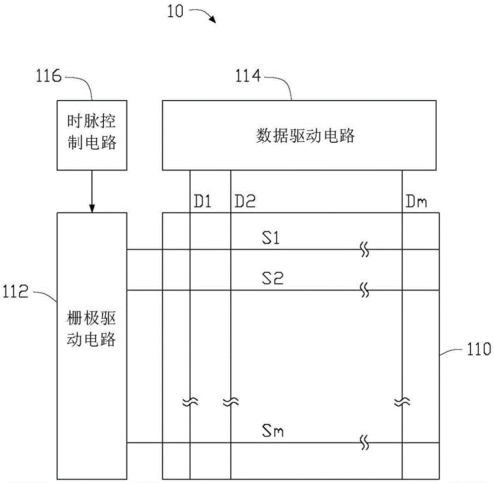
[0015] see figure 1 , figure 1 It is a schematic diagram of the first embodiment of the liquid crystal panel of the present invention. The liquid crystal panel 10 includes a TFT array 110 , a gate driving circuit 112 , a data driving circuit 114 and a clock control circuit 116 . The gate drive circuit 112 and the data drive circuit 114 respectively use the scan line (S1-Sn) and the data line (D1-Dm) to control the thin film transistor array 110 to display the picture, wherein the gate drive circuit 112 is used to open and close and scan The thin film transistors connected with the lines (S1-Sn), the data driving circuit 114 is used to write data into the corresponding thin film transistors of the thin film transistor array 110 through the data lines (D1-Dm). The liquid crystal display panel 10 may be, but not limited to, an in-plane switching (In-Plane Switching, IPS) panel, a fringe field switching (Fringe Field Switching, FFS) panel, and the like.

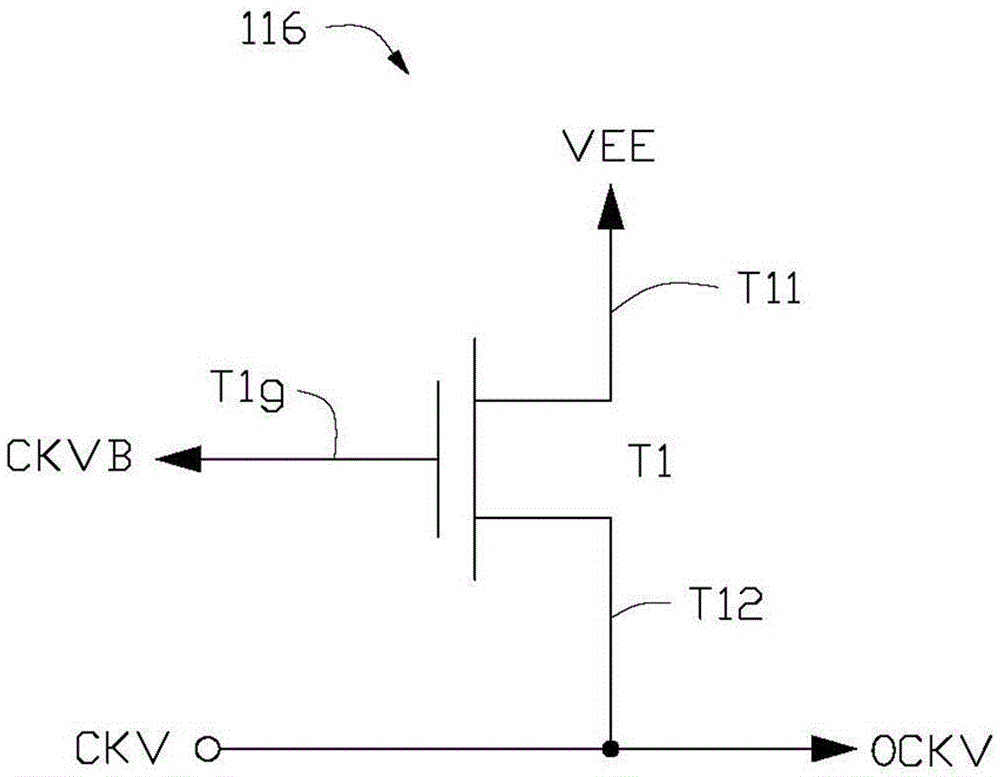
[0016] Please also ref...


PUM


Abstract

The invention provides a liquid crystal display panel, comprising a plurality of scanning lines which are arranged in parallel, a grid electrode driving circuit and a clock pulse control circuit. The pulse control circuit receives clock pulse signals and performs angle cutting on the clock pulse signal under the control of control signals to form clock pulse output signals; the clock pulse control circuit outputs the clock pulse output signal to the grid electrode driving circuit; and the grid electrode driving circuit utilizes the clock pulse output signal as the grid electrode driving signal in order to drive the plurality of scanning lines.

Description

technical field [0001] The invention relates to a liquid crystal panel. Background technique [0002] The liquid crystal panel includes a gate driving circuit that outputs a gate driving signal to sequentially turn on thin film transistors (ThinFilm Transistor, TFT) on the scanning line. Usually the gate driving signal is a square wave signal, but due to process factors, there will be parasitic capacitance and resistance on the scanning line, which will cause RC delay, resulting in waveform distortion and flicker on the LCD panel. Contents of the invention [0003] In view of this, it is necessary to provide a liquid crystal panel that reduces screen flicker. [0004] A liquid crystal panel includes a plurality of scanning lines arranged in parallel, a gate drive circuit and a clock control circuit. The clock control circuit receives the clock signal, and under the control of the control signal, cuts the angle of the clock signal to form a clock output signal. The clock...

Claims


Application Information

Patent Timeline
Patent Type & Authority Applications(China)
IPC IPC(8): G09G3/36
CPCG09G3/3611G09G3/3677G09G2310/067G09G2320/0219G09G2320/0223G09G2320/0247
Inventor 王明宗黄嘉桦梅文淋王慧
Owner CENTURY DISPLAY (SHENZHEN) CO LTD
Why Eureka
Try Eureka