Manufacturing method of optical microstructure, processing machine cabinet and light guide plate die

An optical microstructure and manufacturing method technology, applied in the directions of light guides, optics, optical components, etc., can solve the problem of the decrease in the processing yield of optical microstructures, the influence of the shape or size of optical microstructures, and the inability of a single-mode structure to meet the requirements of light guiding efficiency and other problems, to achieve the effect of improving imprint yield, optimal structural strength and variability

Inactive Publication Date: 2015-12-09
SHANGHAI XIANGLONG ELECTRONICS TECH
View PDF5 Cites 8 Cited by
  • Summary
  • Abstract
  • Description
  • Claims
  • Application Information

AI Technical Summary

Problems solved by technology

Especially during the embossing process, because the rollers must exert a certain pressure on the light guide plate, after a long period of pressing, the wrinkled dots are prone to cracking due to force. Bending or collapsing and falling into the wrinkled dots, reducing the processing life of the substrate or mold core
Moreover, the shape or size of the optical microstructure on the surface of the light guide plate made by embossing through this kind of substrate will be affected, resulting in a decrease in the processing yield of the optical microstructure of the light guide plate.
[0007] In addition, the corrugated dots formed on the mold core or the substrate through laser processing are in the form of depressions, which limits the shape of the optical microstructure of the light guide plate after being molded by the mold core or the substrate.
With the expansion of the application scope of the light guide plate, a single shape structure can no longer meet the more diverse light guide performance requirements, so how to adjust and improve the shape and processing process of the corrugated dots on the mold core or substrate used to manufacture the light guide plate , and the service life of the mold core or substrate, etc., are one of the subjects that need to be improved at present.

Method used


Image

  • Manufacturing method of optical microstructure, processing machine cabinet and light guide plate die
  • Manufacturing method of optical microstructure, processing machine cabinet and light guide plate die
  • Manufacturing method of optical microstructure, processing machine cabinet and light guide plate die

Examples


Embodiment 1

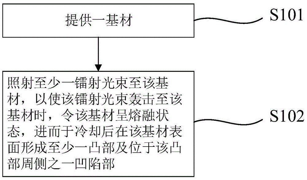
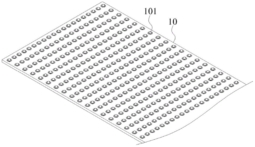
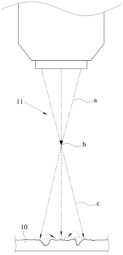
[0053] See figure 1 , 2 And 3 to 4, which are the schematic diagrams of the step flow of the embodiment 1 of the present invention, the three-dimensional schematic diagrams of the substrate after processing, and the schematic diagrams of each processing. The invention discloses a method for manufacturing an optical microstructure, which includes the following steps.

[0054] First, a substrate 10 is provided, which is step S101. Wherein, the substrate 10 has a melting point temperature C 1 . Next, as shown in step S102, at least one laser beam 11 is irradiated to the substrate 10, so that when the laser beam 11 hits the substrate 10, the substrate 10 is in a molten state, and then the substrate 10 is in a molten state after cooling. The surface of the material 10 is formed with at least one convex portion 101 and a concave portion 102 on the peripheral side of the convex portion 101. Wherein, the laser beam 11 has a processing temperature C 2 , And meet C 1 ≤C 2 ≤(1.1×C 1 ), by...


PUM


Abstract

The invention provides a manufacturing method of an optical microstructure, a processing machine cabinet and a light guide plate die. The method is characterized in that a laser beam irradiates a substrate having a melting temperature and one processing temperature of the laser beam meets a condition that C2 is larger than or equal to C1 and is smaller than or equal to (1.1*C1); and when the laser beam bombards the substrate, the substrate is melted down and then is cooled, and thus at least one protrusion part and a recessed part arranged at the peripheral side of the protrusion part are formed on the surface of the substrate. Therefore, the protrusion part can be formed on substrate based on laser processing by controlling the processing temperature. The substrate can be used as a manufacturing die of a light guide plate and coats the outer side of a roller to carry out pressing processing on the light guide plate, so that a recessed microstructure is formed on the surface of the light guide plat by corresponding to the protrusion part and the protrusion part is not easy to crack during the pressing application process. The structure strength is excellent; and the service life of the die can be prolonged.

Description

Technical field [0001] The invention relates to the processing field of light guide plates, in particular to the processing field of manufacturing light guide plates with optical microstructures. Background technique [0002] The light guide plate is a component used in the backlight module to guide light to form a uniform light output. It uses the principle of total reflection to transfer the light incident from the light entrance surface of the light guide plate to the remote end of the light guide plate, and utilizes the plural optical microstructures of the light guide plate The total reflection is destroyed to adjust the light output and the light uniformity to form a uniform surface light source. [0003] The traditional way of forming optical microstructures on the light guide plate is mostly printing. It prints the designed optical microstructure pattern on the light guide plate using the high-dispersion light source material printing material to form dots, and the dots de...

Claims


Application Information

Patent Timeline
Patent Type & Authority Applications(China)
IPC IPC(8): G02B6/00
CPCG02B6/0065G02B6/0015G02B6/0043
Inventor 叶钧皓
Owner SHANGHAI XIANGLONG ELECTRONICS TECH
Why Eureka
Try Eureka