
Detection method for bridging position in metal hard mask all-in-one etching

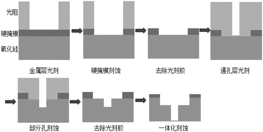
A technology of metal hard mask and detection method, which is applied in the photoengraving process of the pattern surface, the original for photomechanical processing, optics and other directions, and can solve the problems of bridging and the like

Active Publication Date: 2015-12-09
SHANGHAI HUALI MICROELECTRONICS CORP
View PDF6 Cites 5 Cited by
  • Summary
  • Abstract
  • Description
  • Claims
  • Application Information

AI Technical Summary

Problems solved by technology

If the layout requires the size to be the minimum design rule, bridging will occur

Method used


Image

  • Detection method for bridging position in metal hard mask all-in-one etching
  • Detection method for bridging position in metal hard mask all-in-one etching
  • Detection method for bridging position in metal hard mask all-in-one etching

Examples


Embodiment Construction

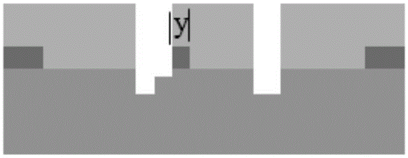
[0035] Please also see Figure 3 to Figure 9 , the detection method of the bridging position in the integrated etching of the metal hard mask in this embodiment specifically includes the following steps:

[0036] Step S01 , providing a layout to be etched with a metal hard mask.

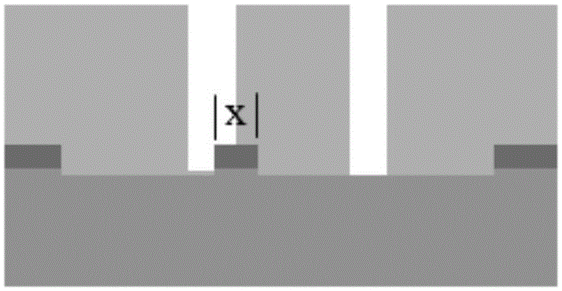
[0037] Step S02, import the optical proximity effect correction result of the metal layer in the layout, and simulate it to obtain the simulated pattern of the metal layer after photolithography, such as Figure 4 As shown, the spacing between adjacent metal layers at A after simulated photolithography is 100 nm.

[0038] Wherein, the optical proximity effect correction result of the metal layer can be obtained according to the prior art. In this embodiment, simulation is preferably carried out according to the correction result of the optical proximity effect of the metal layer and the target result of the photolithography of the metal layer, that is, the theoretical result, to obtain a simulation...


PUM


Abstract

The invention discloses a detection method for a bridging position in metal hard mask all-in-one etching. Through introducing through hole layer etching simulated patterns, which are subjected to optical proximity effect correction and actual etching variation adjustment, of related through hole layers in metal hard mask all-in-one etching into metal layer etching simulated patterns, which are subjected to optical proximity effect correction and actual etching variation adjustment, of metal layers, and merging the etching simulated patterns of the metal layers and the through hole layers, the space between each related through layer and the adjacent metal layers can be judged, so that whether the position with a bridging risk exists or not in the overall metal hard mask all-in-one etching is detected to correct the position before a mask is manufactured.

Description

technical field [0001] The invention relates to the technical field of optical proximity effect correction for semiconductor integrated circuits, in particular to a method for detecting bridge positions in integrated etching of metal hard masks. Background technique [0002] As integrated circuit design and manufacturing enter the ultra-deep sub-micron stage, the deformation and distortion of lithography patterns caused by optical proximity effects seriously affect circuit performance and product yield, such as the size difference between the same pattern in a dense environment and an isolated environment, the key Dimensional graphic breaks or bridges, etc. In order to solve the above problems, an effective method is optical proximity correction. Pattern size and spacing are checked during optical proximity correction and alerted to process weaknesses that are out of specification. [0003] The metal hard mask integrated etching (metalhardmaskallinone) process is widely us...

Claims


Application Information

Patent Timeline
IPC IPC(8): G03F1/36
Inventor 张浩张辰明魏芳吕煜坤朱骏张旭升
Owner SHANGHAI HUALI MICROELECTRONICS CORP
Learn More