Memorizer testing device and memorizer chip testing method

A technology for memory testing and memory chips, applied in static memory, instruments, etc., can solve the problems of not recording information effectively, affecting the test speed, expensive AFM, etc., and achieve the effect of improving the utilization rate and test speed

Active Publication Date: 2015-12-09
SHANGHAI HUALI MICROELECTRONICS CORP
View PDF6 Cites 19 Cited by
  • Summary
  • Abstract
  • Description
  • Claims
  • Application Information

AI Technical Summary

Problems solved by technology

[0003] 1. Due to the one-to-one correspondence between AFM and DUT addresses, this requires the same capacity of AFM and DUT, which makes AFM very expensive
[0004] 2. In general, the failure address of a DUT is much smaller than its capacity, and the traditional failure address storage method, even if only one bit (Bit) of the tested DUT fails, AFM must specially set aside a space equal to the capacity of the DUT To correspond with the DUT one by one, and carry out the identification operation of all addresses of the DUT, so that the information is not effectively recorded in the AFM, and the utilization rate of the AFM hardware storage space is very low
thus greatly affecting the test speed

Method used


Image

  • Memorizer testing device and memorizer chip testing method
  • Memorizer testing device and memorizer chip testing method
  • Memorizer testing device and memorizer chip testing method

Examples


Embodiment Construction

[0035] In order to make the purpose and features of the present invention more obvious and understandable, the specific implementation of the present invention will be further described below in conjunction with the accompanying drawings. However, the present invention can be implemented in different forms and should not be limited to the described embodiments.

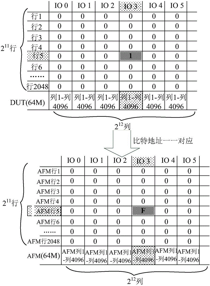
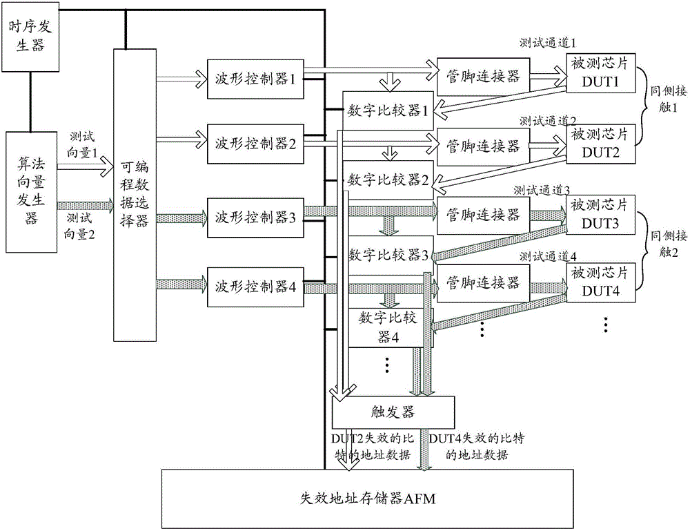
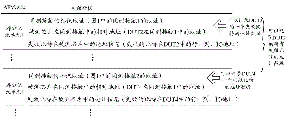
[0036] With the continuous progress of semiconductor technology, those large memories that originally existed in the wafer will be transformed into dozens or hundreds of small memory arrays, and are scattered in every corner of the wafer. The technical solution of the present invention is mainly aimed at improving the problems of low efficiency of failure address information collection and poor utilization of AFM hardware during the large-scale simultaneous testing process of such large-scale memories (flash memory, SRAM, DRAM, etc.). Please refer to Figure 4 As shown, since a memory wafer often has a plurality of me...


PUM


Abstract

The invention provides a memorizer testing device and a memorizer chip testing method. The relation that address spaces of invalid address memorizers of traditional memorizer testing instruments correspond to address spaces of tested chips one to one is changed. The address spaces of the invalid address memorizers are segmented into continuous stored record units. Each stored record unit does not store address data of bits passing tests any more and only stores address data of bits failing to pass the tests, including home addresses of quad-side contact where the stored invalid bits are located, relative addresses in the quad-site contact where the invalid bits are located in chips, address information in the chips where the invalid bits are located and the like. In this way, in the memorizer function testing process, invalid information of multiple chips are stored at the same time, and the utilization rate and the testing speed of invalid address hardware storage spaces are greatly increased.

Description

technical field [0001] The invention relates to the technical field of semiconductor testing, in particular to a memory testing device and a memory chip testing method. Background technique [0002] The birth of chips (or integrated circuits, ICs) has prompted human society to enter a colorful era of digitization, informationization, and intelligence. Computers, mobile phones, digital cameras, high-definition digital TVs, automotive electronic controls, navigation systems, medical equipment, ordnance equipment... Chips are everywhere. In the process of rapid development of chips towards high integration (LSI, VLSI), high speed, and high performance, human pursuit of perfect chips is becoming more and more intense. However, in the real world, in the design, processing, manufacturing and production of integrated circuits, errors (Error) caused by various human and non-human factors are unavoidable. The waste of resources, dangerous accidents, personal casualties caused by the...

Claims


Application Information

Patent Timeline
Patent Type & Authority Applications(China)
IPC IPC(8): G11C29/56
Inventor 李强席与凌王继华高金德
Owner SHANGHAI HUALI MICROELECTRONICS CORP
Why Eureka
Try Eureka