High-rise thick-copper circuit board and manufacturing process

A circuit board manufacturing and circuit board technology, which is applied in the field of image processing, can solve problems such as lamination slides, copper foil wrinkling, resin voids, etc., and achieve the effect of avoiding breakage and ensuring the uniformity of lamination thickness

Inactive Publication Date: 2015-12-16
江西景旺精密电路有限公司
View PDF9 Cites 6 Cited by
  • Summary
  • Abstract
  • Description
  • Claims
  • Application Information

AI Technical Summary

Problems solved by technology

The laminated structure of high-layer thick copper circuit boards involves the lamination of multiple inner-layer thick copper ...

Method used


Image

  • High-rise thick-copper circuit board and manufacturing process
  • High-rise thick-copper circuit board and manufacturing process
  • High-rise thick-copper circuit board and manufacturing process

Examples


Embodiment Construction

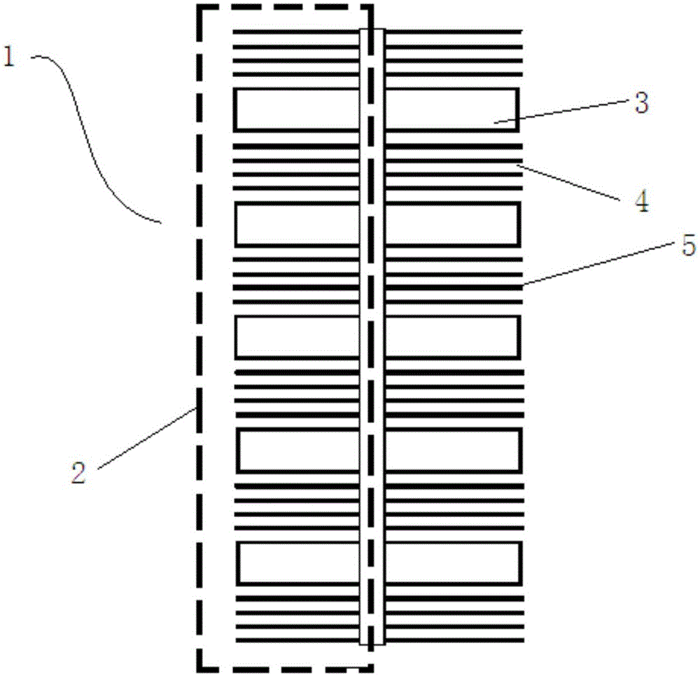
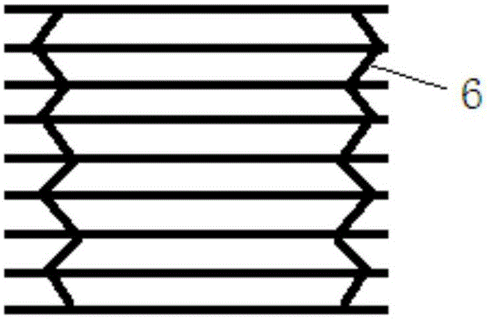
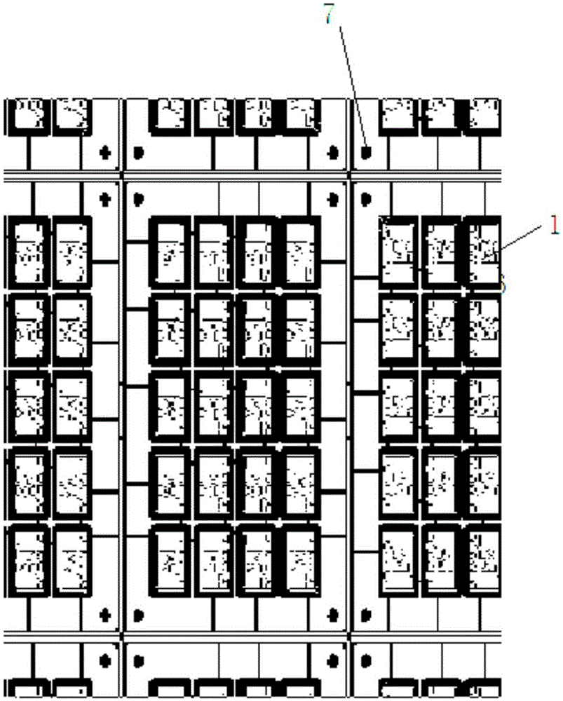
[0029] The present invention will be further described below in conjunction with the accompanying drawings and specific embodiments, but not as a limitation of the present invention.

[0030] The following will clearly and completely describe the technical solutions in the embodiments of the present invention with reference to the accompanying drawings in the embodiments of the present invention. Obviously, the described embodiments are only some, not all, embodiments of the present invention. Based on the embodiments of the present invention, all other embodiments obtained by persons of ordinary skill in the art without creative efforts fall within the protection scope of the present invention.

[0031] It should be noted that, in the case of no conflict, the embodiments of the present invention and the features in the embodiments can be combined with each other.

[0032] The present invention will be further described below in conjunction with the accompanying drawings and s...


PUM


Abstract

The invention relates to the technical field of image processing, especially to a design method of a press-fit laminated structure of a high-rise thick-copper printed circuit board. According to the design, first type high-cementing prepregs are connected and stacked and second type high-cementing prepregs are arranged at intervals. Therefore, a structural design of utilization of all firs type/second type high-cementing prepregs can be avoided; a phenomenon that stability of the circuit board body is affected due to large substrate zone collapsing caused by superposition of multiple prepregs with the same type can be prevented; and board breaking and separation among layers can be avoided. Because the high-rise thick-copper circuit board uses multiple high-resin-content prepregs, the resin recession amount is larger than that of the conventional multi-layer circuit board; and thus S-shaped flow-blocking copper blocks are arranged at the edge of the circuit board body, colloid overflowing during the press-fit process can be prevented.

Description

technical field [0001] The invention relates to the technical field of image processing, in particular to a method for designing a laminated laminated structure of a high-layer thick copper printed circuit board. Background technique [0002] High-layer thick copper printed circuit board is a special type of high-end printed circuit board. Its main features are: the number of layers is generally 10 to 12 layers, and the thickness of copper foil on the inner substrate is 102.9um (3 ounces / ft2) to 137.2 um (4 oz / ft2), high reliability requirements. At present, improving the heat dissipation capacity of printed circuit boards is achieved by design schemes such as wide wires, thick copper foil, multi-layer board structure, large-area copper laying or inner core board design with thick copper foil layer, adding metal base board, and increasing heat conduction holes. , due to the high-density, light, thin, and miniaturized development of electronic products, the development of pr...

Claims


Application Information

Patent Timeline
IPC IPC(8): H05K1/02H05K3/46
CPCH05K3/4611H05K3/4632H05K3/4697H05K2201/042H05K2203/068
Inventor 柯勇谭小林胡定益
Owner 江西景旺精密电路有限公司
Why Eureka
Try Eureka