Silicon nanowire pressure sensor and its packaging structure based on giant piezoresistive properties

A pressure sensor and silicon nanowire technology, applied in the field of micro-nano electromechanical system sensor design, can solve the problems of damage to the sensor chip, only about kilohertz, and small resistance strain coefficient of silicon varistor, so as to eliminate the parasitic latch-up effect. , reduce mechanical stress, the effect of small parasitic capacitance

Active Publication Date: 2018-05-29
南京瑞菲科机电科技有限公司
View PDF6 Cites 0 Cited by
  • Summary
  • Abstract
  • Description
  • Claims
  • Application Information

AI Technical Summary

Problems solved by technology

[0003] However, the silicon cup structure also has the following problems: (1) The quality of the stress film is a key factor determining many characteristics of the sensor
However, on the one hand, the light weight of the stress film will easily lead to a low response rate of the sensor, and the resonance frequency is usually only about kilohertz, which limits the application of the sensor. On the other hand, it also leads to a decrease in the linearity of the pressure sensor. (2) In the traditional silicon piezoresistive pressure sensor, due to the limitation of the manufacturing process, the piezoresistor and its bridge connection circuit are usually arranged on the outer surface of the silicon membrane and exposed to the external environment. During the working process of the device, due to the influence of acid and alkali substances in the external environment, suspended dust, electrostatic particles, etc. on the piezoresistor, it is easy to reduce the performance and service life of the device, affect the long-term reliability of the sensor, and even damage the sensor chip; (3 ) The resistance gauge coefficient of silicon piezoresistors processed by traditional bulk is about 100
The resistance gauge coefficient of silicon varistors with traditional doping process is small. As the size of the sensor becomes smaller, the varistors with traditional doping process can no longer meet the requirements of modern ultra-high sensitivity detection, especially for biochemical pressure sensors with ultra-high sensitivity. Requirements for micro-volume ultrafast detection

Method used


Image

  • Silicon nanowire pressure sensor and its packaging structure based on giant piezoresistive properties
  • Silicon nanowire pressure sensor and its packaging structure based on giant piezoresistive properties
  • Silicon nanowire pressure sensor and its packaging structure based on giant piezoresistive properties

Examples


Embodiment Construction

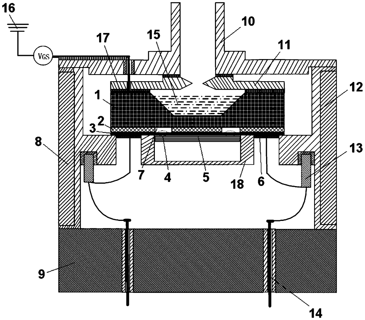
[0038] The present invention will be further described below in conjunction with the accompanying drawings.

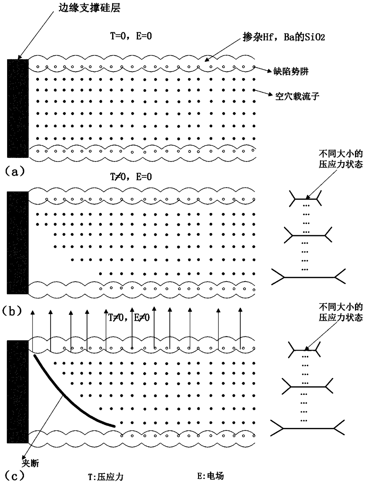
[0039] like figure 1 As shown in (a), the concentration of surface defect states at the interface can be increased by 2 orders of magnitude by doping Hf, Ba and other atoms at the interface between silicon nanowires and surface silicon dioxide, from the original 10 10 cm -2 Surface concentration increased to 10 12 cm -2 Above, due to the low doping concentration of silicon nanowires (generally 10 17cm -2 (below), so the ratio of the concentration of defect states on the surface of silicon nanowires to the concentration of conductive holes on the nanowires is significantly increased, and the effect of defect states is also significantly enhanced. By optimizing the design of the silicon nanowire pressure sensor chip, different compressive stresses can be formed in the silicon nanowire. like figure 1 As shown in (b), under the action of the mechanical compressive s...


PUM

PropertyMeasurementUnit
thicknessaaaaaaaaaa
thicknessaaaaaaaaaa
thicknessaaaaaaaaaa

Abstract

The invention discloses a silicon nanowire pressure sensor based on giant piezoresistive characteristics and its packaging structure, comprising: a shell, a sensor chip, and the sensor chip includes: a silicon nanowire giant piezoresistive sensitive structure, a silicon bottom layer, an insulating two Silicon oxide layer, silicon top layer; the silicon nanowire giant piezoresistive sensitive structure includes multiple silicon nanowires, a stressed and strained film layer, and multiple electrodes, and the multiple silicon nanowires include four pairs of two silicon nanowires arranged in parallel. Nanowires, the four pairs of two silicon nanowires arranged in parallel are respectively connected between the four electrodes and the stressed and strained film layer; the silicon nanowires are provided with through grooves at the corresponding positions of the insulating silicon dioxide layer. The silicon nanowire pressure sensor and its packaging structure based on the giant piezoresistive characteristics provided by the present invention, through the mechanical stress of the sensor chip caused by the external ambient air pressure, the hole concentration of the silicon nanowire conductive channel is greatly reduced, or even pinched off to achieve a huge pressure sensor. piezoresistive effect.

Description

technical field [0001] The invention relates to a silicon nanowire pressure sensor based on giant piezoresistive characteristics and its packaging structure, belonging to the technical field of micro-nano electro-mechanical system (MEMS / NEMS) sensor design. Background technique [0002] The rapid development of microelectronics and micromachining technology has greatly promoted the progress of sensor technology and greatly expanded the application range of sensors. As the most important type of MEMS products, semiconductor pressure sensors are widely used in many fields such as industrial automation and aerospace. At present, piezoresistive pressure sensors mostly use a silicon cup structure. Under pressure, the stress film of the sensor is elastically deformed, sensed by the change of the piezoresistor, and then the output is obtained and processed by the back-end signal conditioning circuit. Calibrating the pressure value can realize the measurement of the pressure. [0...

Claims


Application Information

Patent Timeline
Patent Type & Authority Patents(China)
IPC IPC(8): G01L1/18B82Y40/00B82Y15/00
Inventor 张加宏杨敏葛益娴赵阳
Owner 南京瑞菲科机电科技有限公司
Why Eureka
Try Eureka