Solder ball positioning and parameter identification method for ball grid array pin chip

A ball grid array and parameter recognition technology, which is applied in image data processing, instrumentation, calculation, etc., can solve the problems of low recognition accuracy, slow recognition speed and poor robustness of BGA chip solder balls

Active Publication Date: 2015-12-23
宁波智能装备研究院有限公司
View PDF7 Cites 16 Cited by
  • Summary
  • Abstract
  • Description
  • Claims
  • Application Information

AI Technical Summary

Problems solved by technology

[0006] In order to solve the problems of poor robustness, low recognition accuracy and slow recognition speed of BGA chip solder balls existing in the existing BGA chip recognition method, the present invention further proposes a solder ball positioning and its parameters for ball grid array pin chips recognition methods

Method used


Image

  • Solder ball positioning and parameter identification method for ball grid array pin chip
  • Solder ball positioning and parameter identification method for ball grid array pin chip
  • Solder ball positioning and parameter identification method for ball grid array pin chip

Examples


specific Embodiment approach 1

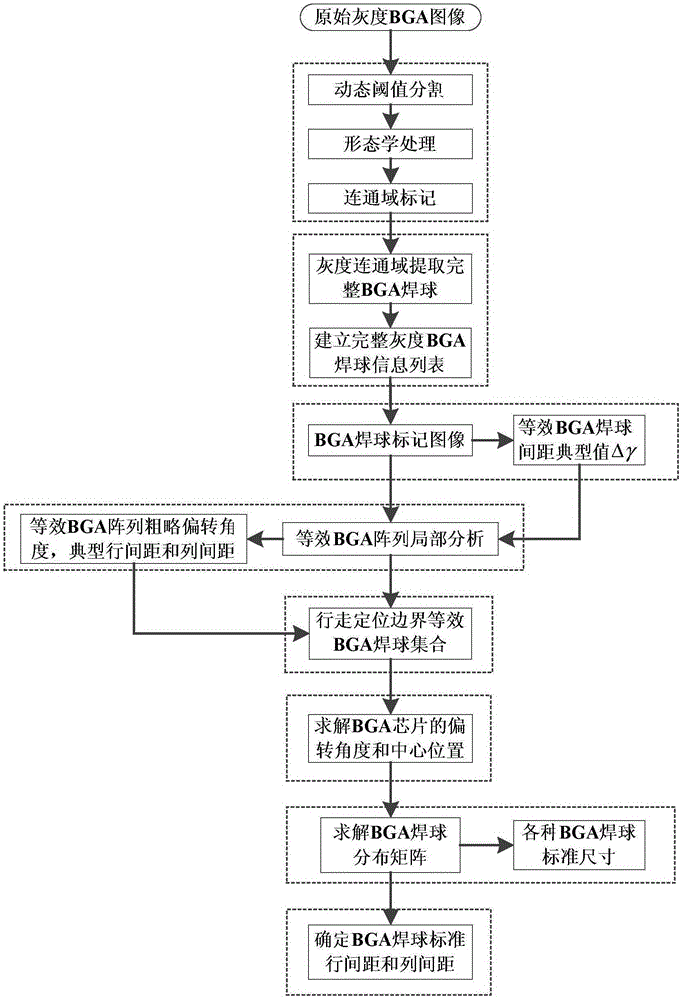
[0048] Specific implementation manner 1: The implementation process of the solder ball positioning and parameter identification method for the ball grid array pin chip described in this embodiment is:

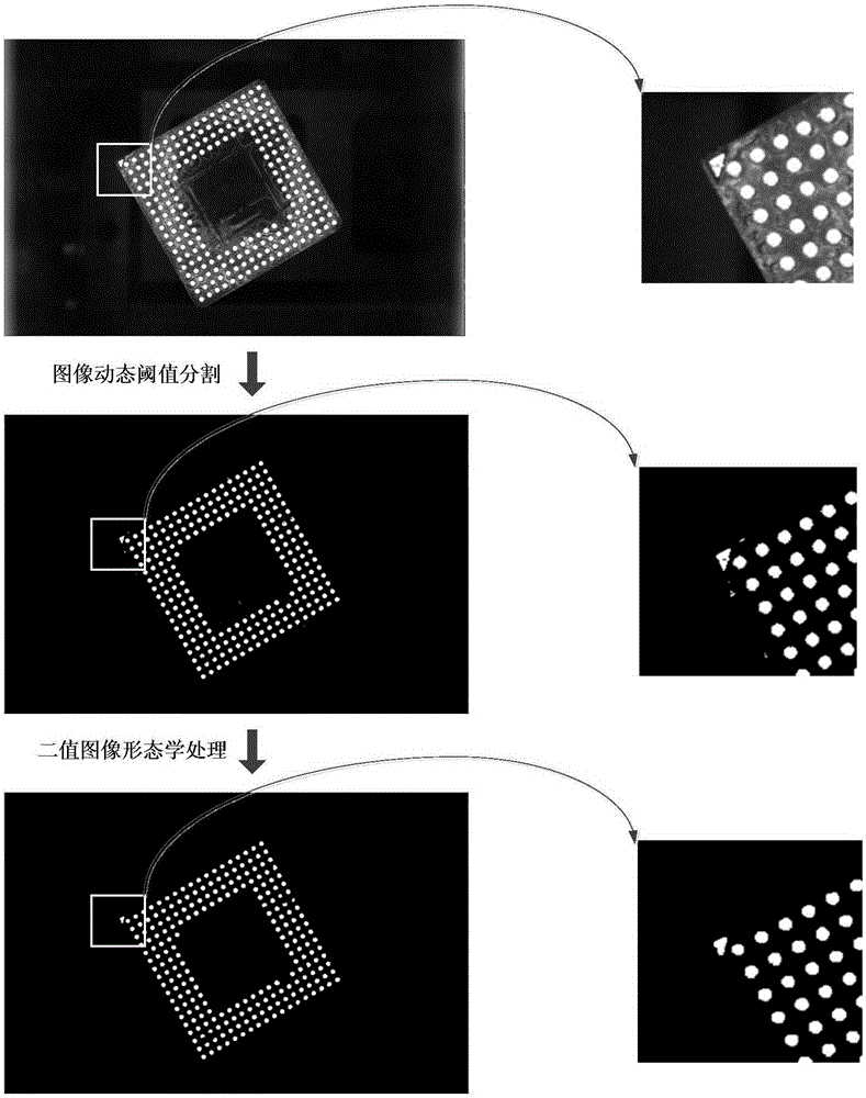
[0049] Step 1: Perform dynamic threshold segmentation on the gray-scale BGA chip image collected by the camera, which is the original image, to obtain a binary solder ball image, and perform morphological opening and closing operations on the binary solder ball image. Each connected domain obtained on the binary solder ball image is recorded as a binary BGA solder ball, and then the connected domain is marked for each binary BGA solder ball;

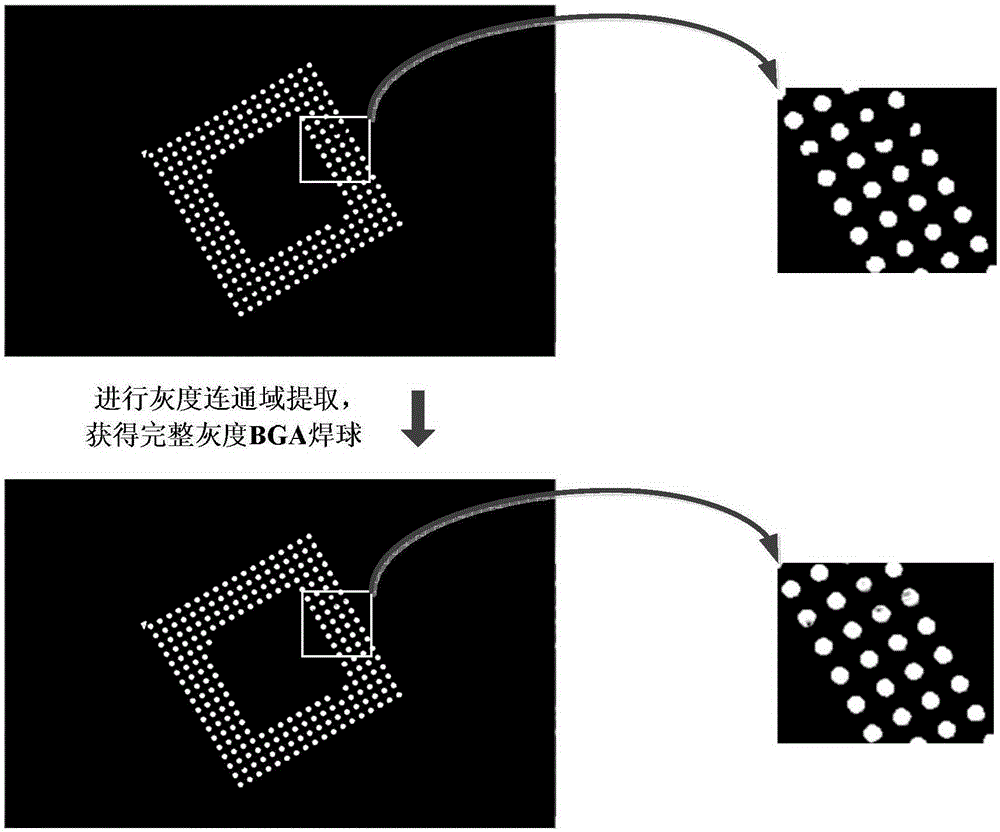
[0050] Step 2: Perform gray-scale connected domain extraction for each binarized BGA solder ball after the connected domain mark obtained in Step 1 in the corresponding neighborhood on the original image to obtain a complete gray-scale BGA solder ball, and establish a complete gray Degree BGA solder ball information list;

[0051] Among them, t...

specific Embodiment approach 2

[0059] Specific implementation manner 2: the following combination figure 2 To illustrate this specific embodiment, this embodiment is a further description of specific embodiment 1. In the steps, the gray-scale BGA chip image collected by a pair of cameras is the original image, and the binary solder ball image is obtained by dynamic threshold segmentation. These operations The specific expression is as follows:

[0060] Among them, the gray-scale BGA chip image undergoes dynamic threshold segmentation to obtain the binary solder ball image I(x,y), which is represented by the following mathematical expression:

[0061] I ( x , y ) = 1 f ( x , y ) ≥ g ( x , y ) + C 0 f ( x , y ) g ( x , y ) + C

[0062] Among them, f(x, y) gray-scale BGA image is the original image; g(x, y) is the image after f(x, y) is average filtered. C is considered to be a constant.

[0063] Compared ...

specific Embodiment approach 3

[0064] Specific implementation manner three: the following combination image 3 This specific embodiment is described. This embodiment is a further description of specific embodiment 1. In step 2, each binarized BGA solder ball obtained in step 1 after being marked with connected domains is within the corresponding neighborhood on the original image Perform gray-scale connected domain extraction to obtain complete gray-scale BGA solder balls, and establish a complete gray-scale BGA solder ball information list, and establish a complete gray-scale BGA solder ball information list. The content includes: the gray contained in each complete gray-scale BGA solder ball Degree pixels, and the center point coordinates of each complete gray-scale BGA solder ball calculated from gray-scale pixels, the smallest outer circle diameter corresponding to each complete gray-scale BGA solder ball, the circumference of each complete gray-scale BGA solder ball, and Roundness; among them, the pixel ...


PUM


Abstract

The invention relates to the vision identification method of a chip, especially to a solder ball positioning and parameter identification method for a ball grid array pin chip. With the method, problems of poor robustness and low chip solder ball identification precision of the existing method can be solved. An original chip image is processed to obtain a binary solder ball image and connected domain marking is carried out on each binary solder ball; grayscale connected domain extraction is carried out on each binary solder ball after the connected domain marking in a corresponding neighborhood range on the original image and a grayscale information list is established; a background image is established and a local analysis is carried out; boundary straight-line fitting is carried out to solve a deflection angle and a center position of the chip; a linear equation of equivalent solder balls at each row and each column is determined, equivalent solder balls searching is carried out to obtain an equivalent solder ball set of each row and an equivalent solder ball of each column, and then correlated dimensions of the solder balls are solved; and linear fitting is carried out, and all fitting straight line spaces at adjacent rows are used as solder ball standard row intervals and fitting straight line spaces of adjacent columns are used as solder ball standard column intervals. For identification and positioning of a chip with a 500-solder-ball-pin scale, the time is less than 200ms.

Description

Technical field [0001] The invention relates to a fast visual recognition method of a ball grid array package chip. Background technique [0002] With the increase in the integration of chips on PCBs, surface mount technology (SMT) is gradually replacing traditional manual soldering and is used in the production process of PCB chip placement. As the core production unit in SMT, the placement machine mainly relies on the vision system Complete the identification, inspection and placement of electronic components, so how to ensure that the chip can be accurately and efficiently identified, detected and positioned through the vision system will directly determine the yield and production efficiency of the final product. [0003] BGA (Ball Grid Array Package) chips are widely used in large-scale integrated circuits due to their high degree of integration and a large number of IO pins. It is precisely because of this characteristic that BGA chips (ball grid array pin chips) are more pr...

Claims


Application Information

Patent Timeline
Patent Type & Authority Applications(China)
IPC IPC(8): G06T7/00
CPCG06T7/0004G06T2207/10004G06T2207/30141G06T2207/30152
Inventor 高会军靳万鑫于金泳杨宪强孙昊白立飞
Owner 宁波智能装备研究院有限公司
Why Eureka
Try Eureka