
Power charging circuit
A charging circuit and power supply technology, applied in battery circuit devices, circuit devices, current collectors, etc., can solve problems such as overcurrent and increased charging current.
Patent Information
- Authority / Receiving Office
- CN · China
- Current Assignee / Owner
- Publication Date
- 2015-12-23
Smart Images
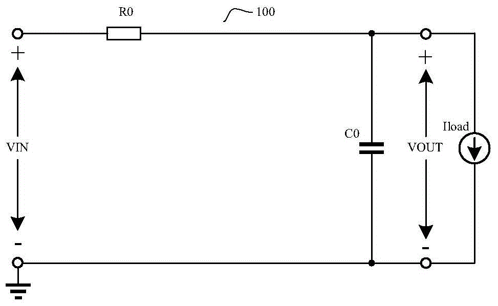
Figure 1 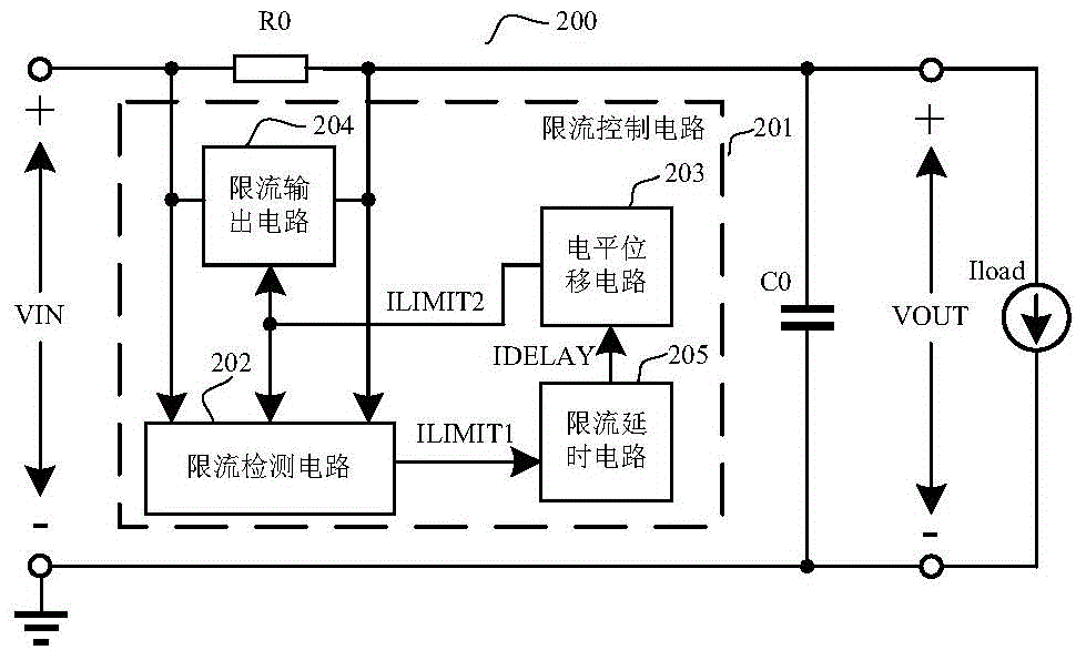
Figure 2 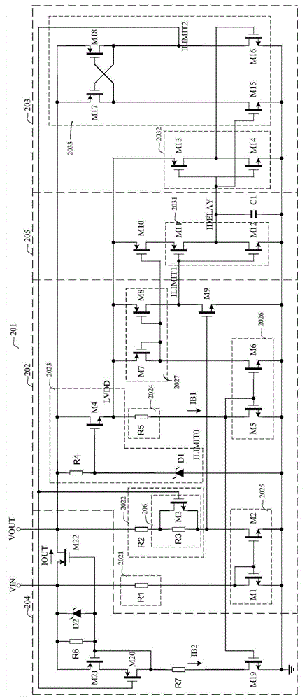
Figure 3
Abstract
Description
technical field
[0001] The invention relates to power charging technology, in particular to a power charging circuit. Background technique
[0002] When various types of power supplies such as switching power supplies are working, they must first charge the output capacitor at the output port of the power supply, and then supply power to the load at the output port after the charging is completed. When the power supply is charging, in order to prevent the output capacitor and other components from being damaged due to excessive charging current, a current-limiting resistor is generally used to limit the charging current.
[0003] refer to figure 1 , figure 1 A schematic circuit structure diagram of a power charging circuit 100 in the prior art is shown. The power charging circuit 100 includes a current limiting resistor R0 and an output capacitor C0, and the power charging circuit is used to provide a load current Iload to a load.
[0004] When charging starts, the input...
Examples
no. 1 example
[0094] refer to figure 2 , figure 2 A schematic circuit structure diagram of the power charging circuit 200 of the first embodiment is shown. The power charging circuit 200 includes a current limiting resistor R0, a current limiting control circuit 201 and an output capacitor C0. The power charging circuit 200 is used to provide a load current Iload to a load.
[0095] Among them, the first terminal of the current limiting resistor R0 is connected to the positive terminal of the input voltage; the first terminal of the output capacitor C0 is connected to the second terminal of the current limiting resistor R0, and the second terminal of the output capacitor C0 is connected to the negative terminal of the input voltage and grounded. The voltage between the positive terminal and the negative terminal of the input voltage is the input voltage VIN, and the voltage across the output capacitor C0 is the output voltage VOUT; the input terminal of the current-limiting control circu...
no. 2 example
[0144] refer to Figure 5 , Figure 5 A schematic circuit structure diagram of the power charging circuit 200 of the second embodiment is shown. The power supply charging circuit 200 of the second embodiment is basically the same as that of the first embodiment, the difference is that the current limiting delay circuit is omitted in the current limiting control circuit 201, and the level shift circuit 203 directly controls the first current generated by the current limiting detection circuit 202. The current limit control signal ILIMIT1 is level-shifted to obtain a second current limit control signal ILIMIT2 .
[0145] refer to Figure 6 , Figure 6 A schematic diagram of a specific circuit structure of the current limiting control circuit 201 according to the second embodiment of the present invention is shown. and image 3 The structure of the first embodiment is basically the same, except that the current-limiting delay circuit and the current-limiting hysteresis circu...
no. 3 example
[0159] refer to Figure 8 , Figure 8 A schematic circuit structure diagram of the power charging circuit 200 of the third embodiment is shown. The power supply charging circuit 200 of the third embodiment is basically the same as the first embodiment, the difference is that the current-limiting hysteresis circuit is omitted in the current-limiting detection circuit 202 of the third embodiment, which can be obtained from Figure 9 Seen in the specific circuit configuration shown.
[0160] about Figure 8 and Figure 9 For the circuit structure shown, reference may be made to the relevant description of the first embodiment, and details are not repeated here.
[0161] refer to Figure 10 , Figure 10 show Figure 9 The working signal waveform of the specific circuit shown. Figure 10 The signals contained in are: input voltage VIN, output voltage VOUT, internal power supply voltage LVDD, first current-limiting control signal ILIMIT1, delay signal IDELAY, second current-...