touch panel
A technology of touch panels and substrates, which is applied in the fields of instruments, calculations, electrical digital data processing, etc., and can solve the problems that nano silver wires are difficult to overcome haze, and too many production equipments are replaced.
- Summary
- Abstract
- Description
- Claims
- Application Information
AI Technical Summary
Problems solved by technology
Method used
Image
Examples
Embodiment Construction
[0035] In order to make the purpose, technical solutions and advantages of the present invention more clear, the present invention will be further described in detail below in conjunction with the accompanying drawings and implementation examples. It should be understood that the specific embodiments described here are only used to explain the present invention, not to limit the present invention.
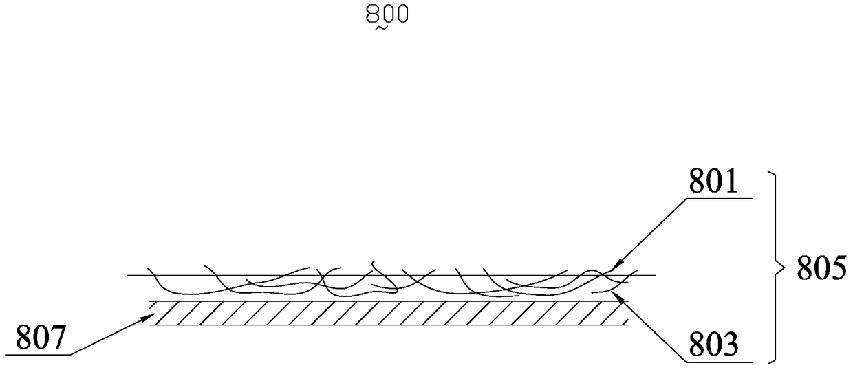
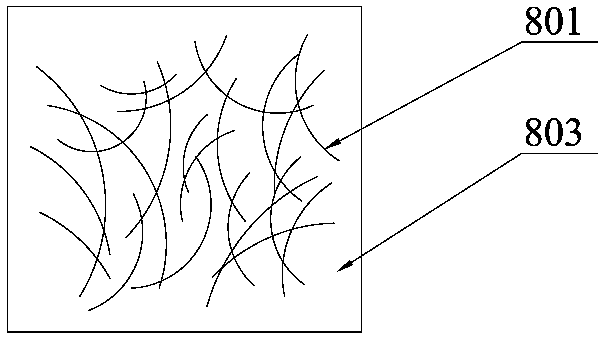
[0036] see figure 1 and figure 2 , is a cross-sectional schematic diagram of a silver nano wire conductive film 800, a transparent conductive layer 805 is generally fabricated on a substrate 807, including a plurality of silver nano wires 801 embedded in a matrix 803, and the silver nano wires 801 are arranged in the matrix 803 overlapping each other to form a conductive network. The wire length of silver nano wires 801 (silver nano wires, referred to as SNW) is 10-300 μm, preferably 20-100 μm, preferably 20-50 μm in length, and the wire diameter (or wire width) of nano silver w...
PUM
 Abstract
Description
Claims
Application Information


