Reverse conducting IGBT device

A reverse-conducting device technology, applied in the field of reverse-conducting insulated gate bipolar transistors and insulated gate bipolar transistors, can solve the problems of poor reverse recovery characteristics, affecting diode conduction characteristics, and reducing reliability, etc. Achieve fast reverse recovery time and eliminate the effect of snapback phenomenon

Inactive Publication Date: 2015-12-30
UNIV OF ELECTRONIC SCI & TECH OF CHINA
View PDF4 Cites 17 Cited by
  • Summary
  • Abstract
  • Description
  • Claims
  • Application Information

AI Technical Summary

Problems solved by technology

However, this method will seriously affect the diode conduction characteristics during reverse freewheeling, has poor re

Method used


Image

  • Reverse conducting IGBT device
  • Reverse conducting IGBT device
  • Reverse conducting IGBT device

Examples


Embodiment Construction

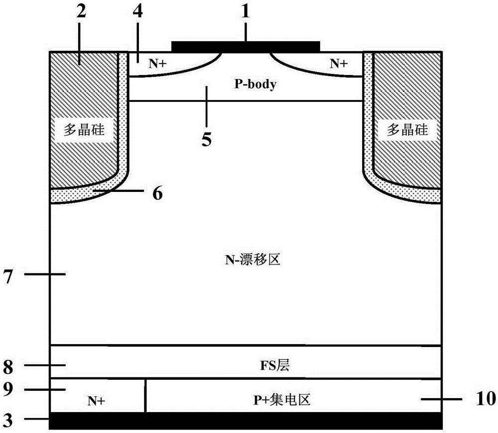
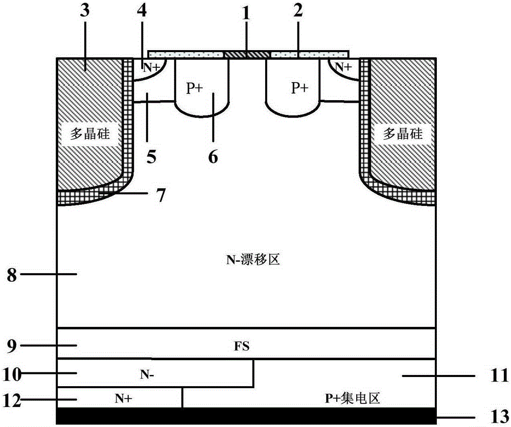
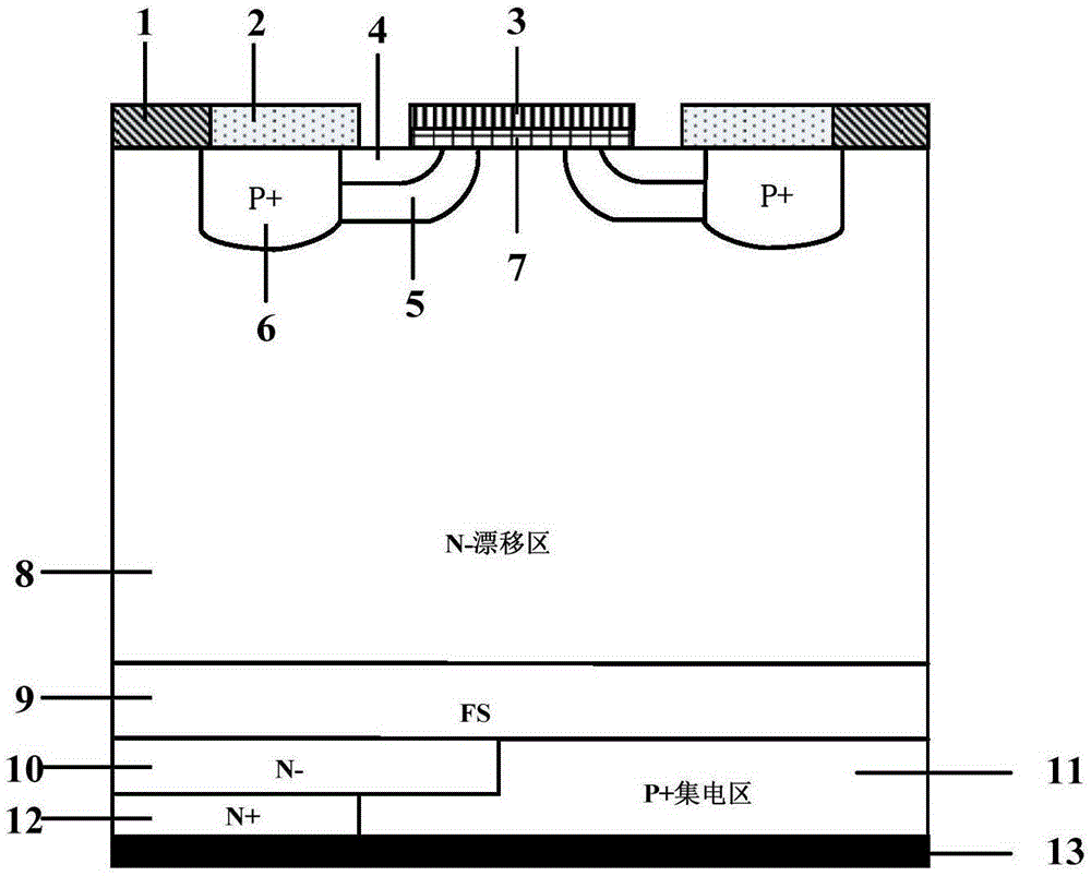
[0024] A reverse conduction type IGBT device of the present invention, such as figure 2 As shown, its cell structure includes an N-drift region 8, an emitter structure and a gate structure located on the upper layer of the N-drift region 8, and a collector structure located on the lower layer of the N-drift region 8; the gate structure is a trench The gate includes a gate oxide layer 7 and a polysilicon gate electrode 3 located in the gate oxide layer 7; the emitter structure is located between two trench gates and includes an emitter metal 2, an N+ emitter region 4, and a P-type base region 5 and P+ region 6; the N+ emitter region 4 is located in the P-type base region 5, and the N+ emitter region 4 and the P-type base region 5 are connected to the gate oxide layer; the P+ region 6 is connected to the P-type base region 5; the The emitter metal 2 is located on the upper surface of the N+ emitter region 4 and the P+ region 6; the collector structure includes a P+ collector re...


PUM


Abstract

The invention belongs to the technical field of power semiconductor devices, and particularly relates to a reverse conducting IGBT device. Compared with a conventional reverse conducting IGBT structure, emission electrode schottky metal is additionally arranged in source electrode metal, and an N-region is arranged below an N-type electric field stop layer so that a reverse recovery characteristic working under a freewheel diode mode is respectively improved and generation of the snapback phenomenon is suppressed. The beneficial effects of the reverse conducting IGBT device are that the reverse conducting IGBT device has short reverse recovery time, the snapback phenomenon can be eliminated at a shorter back P+ collector region, and the preparation technology of the reverse conducting IGBT device is compatible with the technology of the conventional IGBT device. The invention is especially suitable for the reverse conducting IGBT device.

Description

technical field [0001] The invention belongs to the technical field of power semiconductor devices, and relates to an insulated gate bipolar transistor (IGBT), in particular to a reverse conduction type insulated gate bipolar transistor (RC-IGBT). Background technique [0002] Insulated Gate Bipolar Transistor (IGBT) is a new type of power electronic device combining MOS field effect and bipolar transistor. It not only has the advantages of easy driving and simple control of MOSFET, but also has the advantages of low conduction voltage of power transistor, large on-state current and small loss. It has become one of the core electronic components in modern power electronic circuits and is widely used in Various fields of the national economy such as communications, energy, transportation, industry, medicine, household appliances and aerospace. The application of IGBT plays an extremely important role in improving the performance of power electronic systems. [0003] In powe...

Claims


Application Information

Patent Timeline
IPC IPC(8): H01L29/06H01L29/47H01L21/331H01L29/739
CPCH01L29/7397H01L29/0603H01L29/47H01L29/66348
Inventor 李泽宏郭绪阳张明陈文梅伍济陈钱任敏张金平高巍张波
Owner UNIV OF ELECTRONIC SCI & TECH OF CHINA
Why Eureka
Try Eureka