Semiconductor device manufacturing method thereof

A manufacturing method and semiconductor technology, applied in semiconductor/solid-state device manufacturing, semiconductor devices, transistors, etc., can solve problems such as low cost and miniaturization limitations, increase in current value, and increase in the number of components, and achieve device miniaturization, The effect of reducing costs and reducing the number of parts

Inactive Publication Date: 2005-10-05
SANYO ELECTRIC CO LTD
View PDF1 Cites 7 Cited by
  • Summary
  • Abstract
  • Description
  • Claims
  • Application Information

AI Technical Summary

Problems solved by technology

[0020] However, when using an external Schottky barrier diode D sbd When the number of components increases, there are restrictions on low cost and miniaturization
[0021] In MOSFET 200, source region 134 and body region 140 are short-circuited and used, but body region 140 has a high resistance, and a potential difference due to the resistance actually occurs between the source and the body.
When the potential difference is more than 0.6V, there is a problem of parasitic bipolar action between the source-body-drain, and the current value increases sharply until breakdown

Method used


Image

  • Semiconductor device manufacturing method thereof
  • Semiconductor device manufacturing method thereof
  • Semiconductor device manufacturing method thereof

Examples


Embodiment Construction

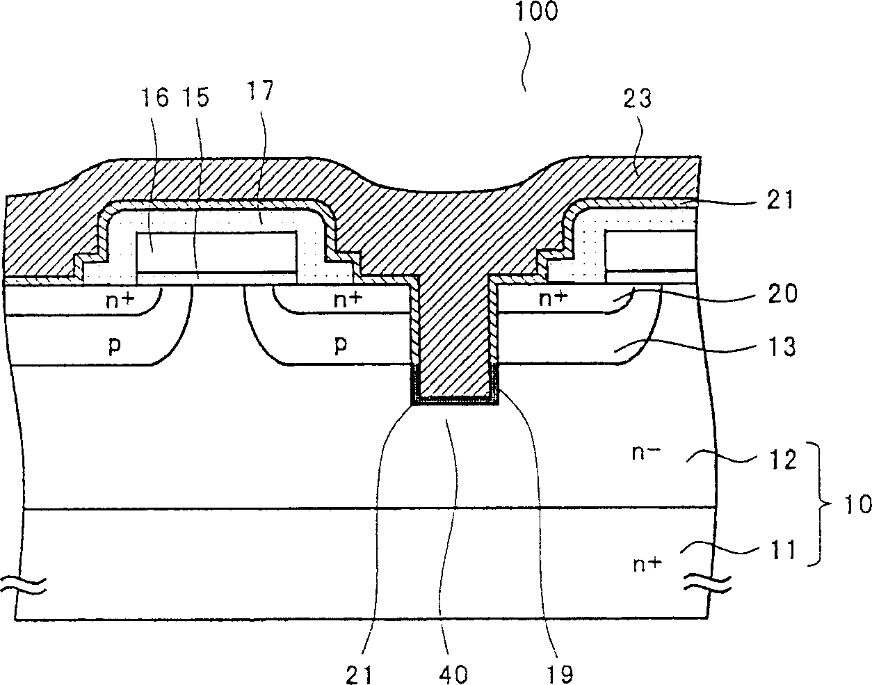
[0076] refer to Figure 1 to Figure 13 The embodiment of the present invention will be described in detail by taking an n-channel MOSFET as an example.

[0077] First, refer to Figure 1 to Figure 5 The first embodiment will be described. figure 1 is a cross-sectional view showing the MOSFET structure.

[0078] The MOSFET 100 is composed of a conductive semiconductor substrate 10 , a channel layer 13 , an insulating film 15 , a gate electrode 16 , a source region 20 , a groove 19 , a first metal layer 21 , and a second metal layer 23 .

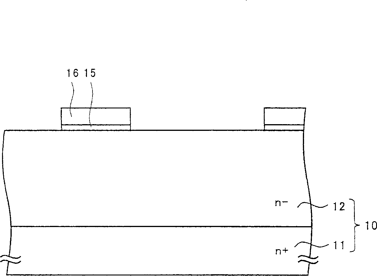
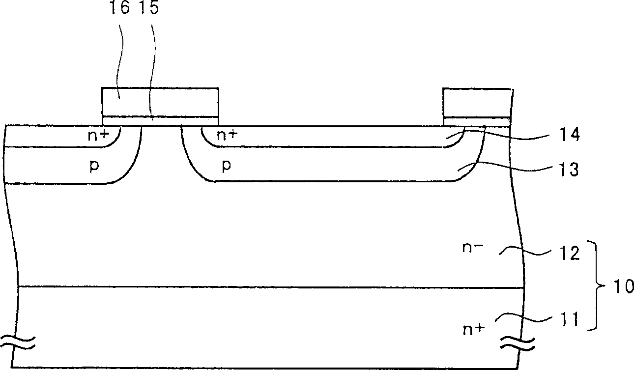
[0079] A conductive type semiconductor substrate 10 is a substrate in which an n-type semiconductor layer 12 is stacked on an n+ type silicon semiconductor substrate 11 by epitaxial growth or the like, and the n-type semiconductor layer 12 constitutes a drain region.

[0080] The channel layer 13 is a p+ type impurity diffusion region provided on the surface of the n-type semiconductor layer 12 , and the source region 20 where phosphorus o...


PUM


Abstract

The invention solves the problem that a device becomes large in size and the number of components increases because a Schottky barrier diode is provided externally, in the case that the MOSFET includes a parasitic pn diode between the source and drain for use as Fast Recovery Diode (FRD), and a pn junction diode becomes a factor for preventing high speed switching operation and low power consumption. A groove is provided through a channel layer between adjacent gate electrodes of the MOSFET and a Schottky metal layer is also provided within the groove. Accordingly, since the bottom of groove is formed with the Schottky barrier diode, the Schottky barrier diode can be comprised within a diffusing region of the MOSFET. Cosequently, reduction in size of device and reduction in the number of components can be realized simultaneously.

Description

technical field [0001] The present invention relates to a semiconductor device and a manufacturing method thereof, and more particularly to a semiconductor device incorporating a Schottky barrier diode in a MOSFET and a manufacturing method thereof. Background technique [0002] Figure 14 Take n-channel type as an example to illustrate the structure of the existing MOSFET. [0003] MOSFET 200 is composed of semiconductor substrate 130 , channel layer 133 , source region 134 , gate oxide film 135 , and gate electrode 136 . [0004] The semiconductor substrate 130 is formed by laminating an n-type epitaxial layer 132 and the like on an n+ type silicon semiconductor substrate 131, and the n-type epitaxial layer 132 constitutes a drain region. [0005] The channel layer 133 is formed on the surface of the semiconductor substrate in the field portion with a dose of 1.0×10 13 ~1.0×10 14 cm -2 Impurity diffusion region set by implanting p+ type ions. [0006] The source regio...

Claims


Application Information

Patent Timeline
Patent Type & Authority Applications(China)
IPC IPC(8): H01L21/336H01L21/338H01L21/8234H01L27/04H01L27/06H01L27/095H01L29/47H01L29/78H01L29/872
CPCH01L29/7806H01L29/66727H01L29/66734H01L29/7813H01L29/872G07F17/3244G07F9/04
Inventor 冈田哲也船越明彦
Owner SANYO ELECTRIC CO LTD
Why Eureka
Try Eureka