

Channel MOS P-N junction Schottky diode structure and manufacturing method thereof
A technology of Schottky diode and channel structure, applied in semiconductor/solid-state device manufacturing, electrical components, circuits, etc., can solve the problems of low forward voltage drop value, consumption of conductive area, etc.
- Summary
- Abstract
- Description
- Claims
- Application Information
AI Technical Summary
Problems solved by technology
Method used
Image

Examples
Embodiment Construction
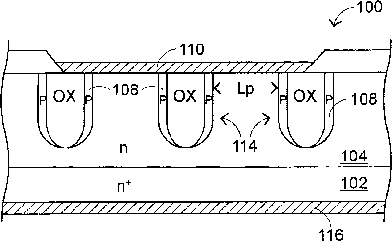
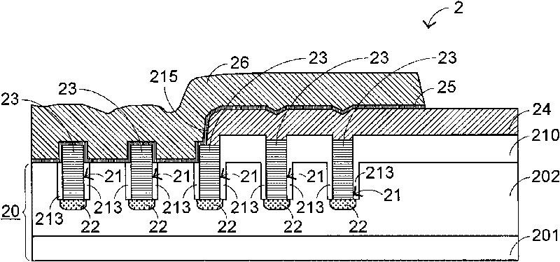
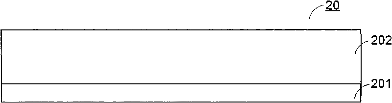
[0101] See figure 2 , which is a schematic diagram of a first preferred embodiment of a trenched metal-oxide-semiconductor P-N junction Schottky diode structure developed by the present invention to improve defects caused by known technical means. We can clearly see from the figure that the trench metal oxide semiconductor P-N junction Schottky diode structure 2 mainly includes a substrate 20, a channel structure 21, an ion implantation region 22, a polysilicon layer 23, an oxide Object layers 213, 210, 24 and metal layers 25, 26, wherein the substrate 20 is composed of a high doping concentration N-type silicon substrate (N+ silicon substrate) 201 and a low doping concentration N-type epitaxial layer (N- epitaxial layer) 202; the channel structure 21 is formed in the substrate 20 and the oxide layer 210, 213; the ion implantation region 22 is formed in the low doping concentration N-type epitaxial layer 202, and is formed in the channel The polysilicon layer 23 in the struc...
PUM
 Abstract
Description
Claims
Application Information