Making process of fast recovery chip

A manufacturing process and chip technology, which is applied to the manufacturing process of fast recovery chips, can solve the problems of high failure rate and low reliability, and achieve the effects of low failure rate, high reliability and improved functional characteristics.

Active Publication Date: 2016-09-28
YANGZHOU HY TECH DEV
View PDF4 Cites 7 Cited by
  • Summary
  • Abstract
  • Description
  • Claims
  • Application Information

AI Technical Summary

Problems solved by technology

[0004] The purpose of the present invention is to provide a manufacturing process for fast recovery chips. The present invention provides a process combination that solves the technical problems of low reliability and high failure rate of products produced in the prior art.

Method used


Image

  • Making process of fast recovery chip
  • Making process of fast recovery chip

Examples


Embodiment 1

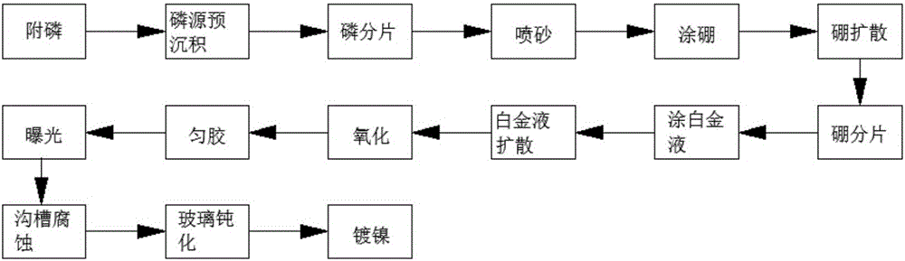
[0037] Such as figure 1 A fast recovery type chip fabrication process shown includes the following steps:

[0038] (1) Phosphorous attachment: first clean the silicon wafers, then sandwich the paper-like phosphorus source with a concentration of not less than 70% between adjacent silicon wafers, and place them on the quartz boat in turn; the silicon wafer cleaning steps are: First put the silicon wafer into the HF solution and soak for 2 minutes, wherein the ratio of the HF solution is HF:H2O=1000ml:8500ml, the temperature is 35°C, and then use the Harmo solution and hot pure water for ultrasonic vibration, the Harmo solution ratio is Harmo powder: H2O=200g: 18000ml, temperature: 85°C, time 20min, finally flushing, shaking with running water, flushing, drying, silicon wafers are cleaned;

[0039] (2) Phosphorus source pre-deposition: send the quartz boat equipped with silicon wafers into a diffusion furnace with a temperature of 600°C to decompose the phosphorus source for 2 ...

Embodiment 2

[0055] Such as figure 1 A fast recovery type chip fabrication process shown includes the following steps:

[0056] (1) Phosphorous attachment: first clean the silicon wafers, then sandwich the paper-like phosphorus source with a concentration of not less than 70% between adjacent silicon wafers, and place them on the quartz boat in turn; the silicon wafer cleaning steps are: First put the silicon chip into the HF solution and soak for 1min, wherein the ratio of the HF solution is HF:H2O=1000ml:8500ml, the temperature is 25°C, and then use the Harmo solution and hot pure water for ultrasonic vibration, the Harmo solution ratio is Harmo powder: H2O=200g: 18000ml, temperature: 75°C, time 10min, finally flushing, shaking with running water, flushing, drying, silicon wafers are cleaned;

[0057] (2) Phosphorus source pre-deposition: send the quartz boat equipped with silicon wafers into a diffusion furnace with a temperature of 550°C to decompose the phosphorus source for 1 hour, ...


PUM


Abstract

The invention provides a making process of a fast recovery chip. The process comprises the following steps: phosphorus attachment, phosphorus source pre-deposition, phosphorus fragmentation, sand blasting, boron coating, boron diffusion, boron fragmentation, platinum liquid coating, platinum diffusion, oxidation, gluing, exposure, groove corrosion, glass passivation and nickel plating. The reverse recovery time of the assembled bridge-type fast recovery chip is shorter than that of a conventional chip, and the fast recovery chip is good in stability and high in client use reliability.

Description

technical field [0001] The invention relates to the technical field of semiconductor devices, in particular to a manufacturing process of a fast recovery chip. Background technique [0002] With the vigorous development of the semiconductor market, customers' demands for our products are also becoming more diversified and require higher reliability. In the current market, among the customers who mainly manufacture electronic circuits such as switching power supplies, modulators, and frequency converters, there is a great demand for fast recovery products, and the requirements for the characteristics of the products are also extremely strict. Therefore, in order to meet customers' demand for high-end products, fast recovery products are different from conventional products in that they have a low reverse recovery time, which requires doping during the grain production process, but in order to ensure that the grain itself has a relatively high High reliability and glass passi...

Claims


Application Information

Patent Timeline
Patent Type & Authority Applications(China)
IPC IPC(8): H01L21/329H01L29/861
CPCH01L29/6609H01L29/861
Inventor 王道强魏庆山
Owner YANGZHOU HY TECH DEV
Why Eureka
Try Eureka