Etching method for external layer of thick copper plate

A thick copper plate and etching technology, which is used in chemical/electrolytic methods to remove conductive materials, electrical components, and printed circuit manufacturing. Effect

Active Publication Date: 2015-12-30
JIANGMEN SUNTAK CIRCUIT TECH
View PDF3 Cites 9 Cited by
  • Summary
  • Abstract
  • Description
  • Claims
  • Application Information

AI Technical Summary

Problems solved by technology

[0003] The present invention aims at the problem that the dense circuit area on the upper surface is not completely etched while the area with fewer circuits is over-etched when the outer layer of the existing thick copper plate is etched, and provides an outer layer etching method for a thick copper plate with good etching uniformity

Method used


Image

  • Etching method for external layer of thick copper plate
  • Etching method for external layer of thick copper plate

Examples


Embodiment

[0016] This embodiment provides a method for etching the outer layer of a thick copper plate, the thickness of the bottom copper of the outer layer of the thick copper plate is 3OZ, and the thick copper plate includes a first surface (ie, a TOP surface) and a second surface.

[0017] According to the existing positive film process, the outer layer circuit is made on the thick copper plate, which includes the following processes in turn: grinding plate → film attachment → exposure → development → electroplating copper → electrotin plating → film stripping → outer layer etching → tin stripping.

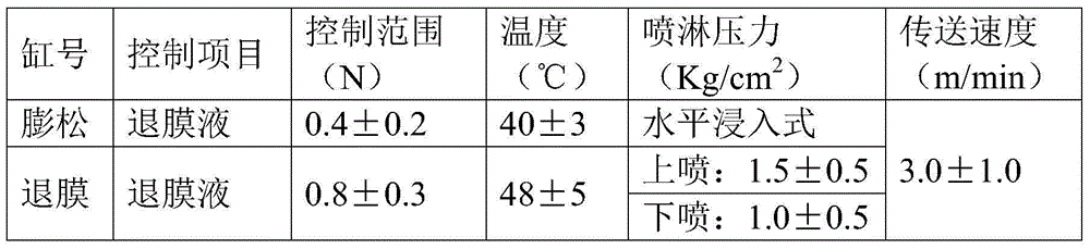
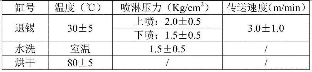
[0018] 1. Before the outer layer is etched, the pre-process is carried out according to the existing technology, as follows: board entry → bulking → film removal → washing → inspection. The process parameters are as shown in the table below (use the film stripping solution commonly used in this field, such as industrial grade sulfuric acid, industrial grade sodium hydroxide).

[0019] ...


PUM


Abstract

The invention relates to an etching method for an external layer of a thick copper plate, and belongs to the technical field of PCB production. Twice etching is used, the up/down orientation of the thick copper plate is changed in the twice etching, each of the two surfaces of the thick copper plate is orientated downwards once and sprayed by an etching solution upwardly, technical parameters including the speed that the thick copper plate passes an etching cylinder, the spraying pressure of the etching solution and the concentration of the etching solution are adjusted, and the adjusted technical parameters cooperate with the twice etching manners, so that the etching uniformity of the external layer of the thick copper plate is high, areas of dense circuits can be cleaned via etching, and areas including fewer circuits are prevented from excessive etching and too thin etching lines. According to the method of the invention, the etching effect for the external layer of the thick copper plate is good.

Description

technical field [0001] The invention relates to the technical field of PCB production and manufacturing, in particular to an outer layer etching method of a thick copper plate. Background technique [0002] The production of PCB (Printed Circuit Board, printed circuit board) generally includes the following processing links: material cutting → negative film process to make inner layer circuit → pressing → drilling → sinking copper → full board electroplating → positive film process to make outer layer circuit → making solder mask Layer → Surface Treatment → Molding. The positive film process also includes grinding plate→filming→exposure→development→copper electroplating→tin electroplating→film removal→outer layer etching→tin removal, in which the outer layer etching generally makes the production board pass through the etching cylinder horizontally, and the upper and lower parts of the production board are A shower head is provided, and the etchant is sprayed to the upper s...

Claims


Application Information

Patent Timeline
Patent Type & Authority Applications(China)
IPC IPC(8): H05K3/06
CPCH05K3/06H05K3/067H05K2203/0786
Inventor 陈广龙白会斌胡志勇
Owner JIANGMEN SUNTAK CIRCUIT TECH
Why Eureka
Try Eureka