Supercharge Your Innovation With Domain-Expert AI Agents!

Memory device

A technology of storage device and flash unit, which is applied in the electronic field, can solve problems such as reducing the lifespan of flash memory, damaging flash memory circuits, and excessive voltage, so as to reduce the average number of write operations and improve life and reliability.

Active Publication Date: 2016-01-13
WUXI ZGMICRO ELECTRONICS CO LTD
View PDF4 Cites 2 Cited by
  • Summary
  • Abstract
  • Description
  • Claims
  • Application Information

AI Technical Summary

Problems solved by technology

[0002] The life of the existing flash memory circuit will be affected by two factors: first, when the flash memory is being written, plugging and unplugging the flash memory may cause excessive voltage and damage the flash memory circuit; second, frequent writing operations will reduce the life of the flash memory

Method used


Image

  • Memory device
  • Memory device

Examples


Embodiment 1

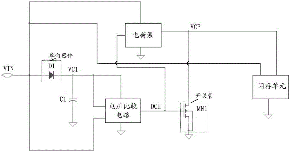
[0022] figure 1 It is a schematic diagram of a storage device provided by Embodiment 1 of the present invention. Such as figure 1 As shown, the storage device includes: a flash memory unit (FlashCell), a charge pump (ChargePump), a switch tube, a voltage comparison circuit (Comparator), a unidirectional device, and a capacitor C1.

[0023] It should be noted that the switching tube may be a switching device such as an NMOS tube, a PMOS tube, a triode, or a thyristor. Unidirectional devices can also have other conversion types, such as diode-connected MOS tubes. In the embodiment of the present invention, the switching transistor is an NMOS transistor MN1, and the unidirectional device is a diode D1 as an example to explain the present invention.

[0024] The power supply voltage VIN is connected to the anode of the diode D1, the cathode of the diode D1 is connected to one end of the capacitor C1, the other end of the capacitor C1 is grounded, the voltage VC1 of the capacito...

Embodiment 2

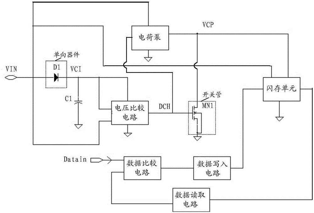
[0033] figure 2 It is a schematic diagram of the storage device provided by Embodiment 2 of the present invention. Such as figure 2 As shown, the device includes: a flash memory unit, a charge pump, a switch tube, a voltage comparison circuit, a unidirectional device, a capacitor C1, a data comparison circuit, a data reading circuit and a data writing circuit.

[0034] Connection relationship reference of power supply voltage VIN, flash memory unit, charge pump, switching device, voltage comparison circuit, unidirectional device and capacitor C1 figure 1 The function of the circuit shown is to prevent the flash memory unit from being over-voltaged and damage the flash memory circuit when the storage device or the flash memory is unplugged, and details will not be described here. Similarly, in the embodiment of the present invention, the switch transistor is the NMOS transistor MN1, and the unidirectional device is the diode D1 as an example to explain the present invention...


PUM


Abstract

The invention relates to a memory device, which comprises a flash memory unit, a charge pump, a voltage comparison circuit, a switch tube, a data reading unit, a data comparison unit and a data writing unit, wherein the flash memory unit is used for storing data; the charge pump is used for boosting power supply voltage and providing work voltage to the flash memory unit; a first input end of the voltage comparison circuit is connected with the power supply voltage; a second input end is coupled to the power supply voltage and is grounded through a capacitor; an output end is coupled to the charge pump; a control end of the switch tube is connected to the output end of the voltage comparison circuit; a first connection end is connected with an output voltage end of the charge pump; a second connection end is grounded; the data reading unit is used for reading existing data of a to-be-written region of the flash memory unit; the data comparison unit is comparing the existing data with the to-be-written data; and the data writing unit is used for writing different parts in the to-be-written data and the existing data into the corresponding region of the flash memory unit and neglecting the same parts in the to-be-written data and the existing data. According to the memory device, the flash memory unit can be protected; damage to the flash memory unit due to over-voltage is avoided; and meanwhile, the lifetime of the flash memory unit can also be further prolonged; and the reliability of the flash memory unit can also be further improved.

Description

technical field [0001] The present invention relates to the field of electronic technology, in particular to a storage device. Background technique [0002] The lifespan of the existing flash memory circuit is affected by two factors: first, when the flash memory is being written, plugging and unplugging the flash memory may cause excessive voltage and damage the flash memory circuit; second, frequent writing operations will reduce the lifespan of the flash memory. In some fields that require long-term work and are inconvenient to repair and replace, such as the Internet of Things field that is getting more and more attention, it is necessary to further improve the life of flash memory circuits. Contents of the invention [0003] The object of the present invention is to provide a kind of memory device for the defect of prior art, can realize the protection to flash memory unit, avoid the flash memory unit from being damaged by overvoltage, meanwhile, can further improve t...

Claims


Application Information

Patent Timeline
Patent Type & Authority Applications(China)
IPC IPC(8): G11C16/30G11C16/26G11C16/06
CPCY02D10/00
Inventor 王钊
Owner WUXI ZGMICRO ELECTRONICS CO LTD
Features
  • R&D
  • Intellectual Property
  • Life Sciences
  • Materials
  • Tech Scout
  • Unparalleled Data Quality
  • Higher Quality Content
  • 60% Fewer Hallucinations
Learn More