Visible-infrared hybrid imaging detector pixel structure and its preparation method

An imaging detector and pixel structure technology, applied in the field of microelectronics, can solve the problems of large alignment deviation between the infrared image part and the visible light image part, which affects the imaging quality, etc., so as to improve the light utilization rate, improve the imaging quality and reduce the loss Effect

Active Publication Date: 2018-06-26
SHANGHAI INTEGRATED CIRCUIT RES & DEV CENT
View PDF4 Cites 2 Cited by
  • Summary
  • Abstract
  • Description
  • Claims
  • Application Information

AI Technical Summary

Problems solved by technology

[0003] However, in the existing hybrid imaging devices, lenses are used to form two optical paths to sense and image visible light and infrared light respectively, and finally a computer processing system is used to synthesize them together. Due to the separation of the optical paths, the formed infrared image part and visible light image Some of them have large alignment deviations, which seriously affect the imaging quality

Method used


Image

  • Visible-infrared hybrid imaging detector pixel structure and its preparation method
  • Visible-infrared hybrid imaging detector pixel structure and its preparation method

Examples


Embodiment Construction

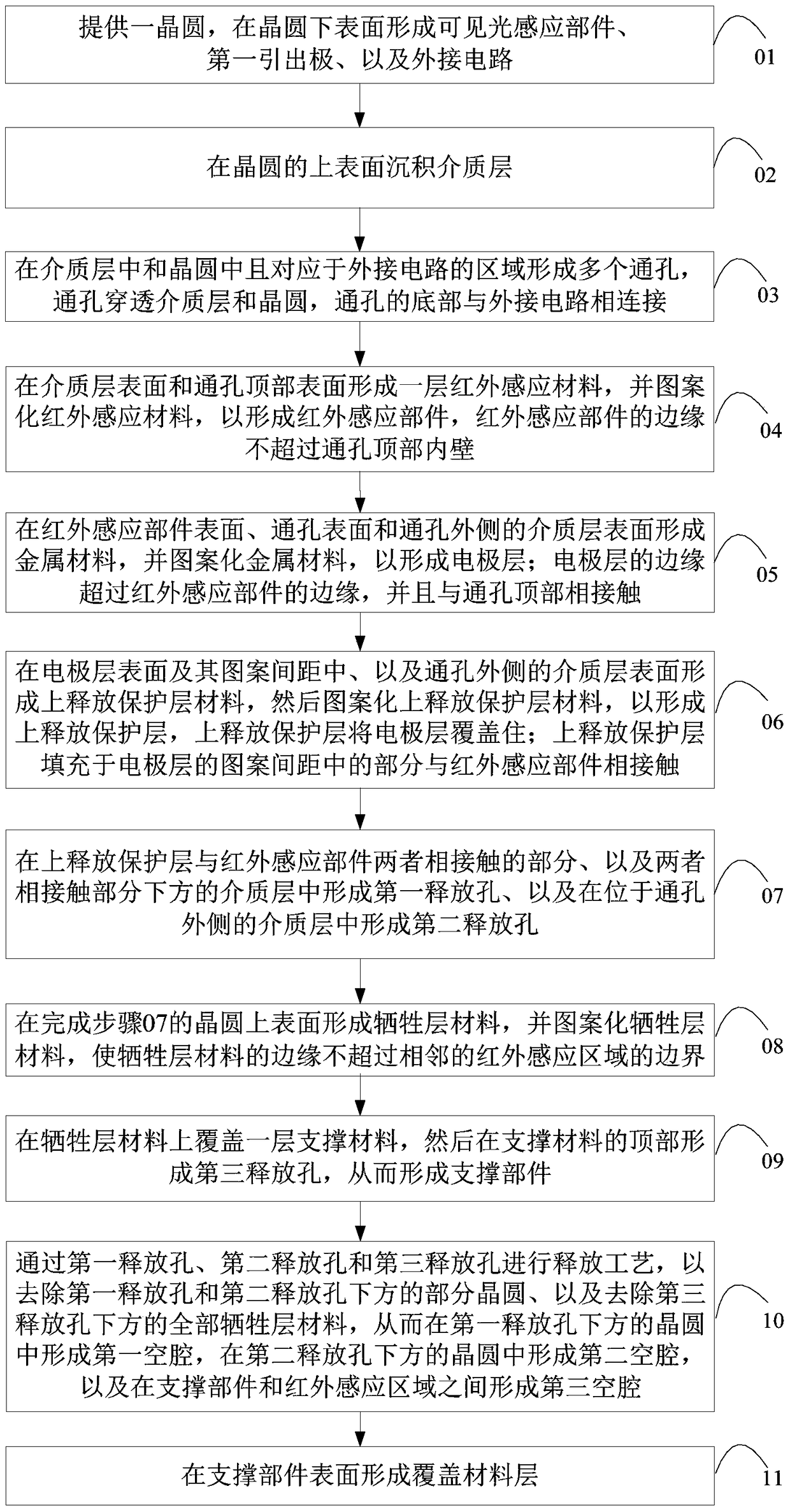
[0046] In order to make the content of the present invention clearer and easier to understand, the content of the present invention will be further described below in conjunction with the accompanying drawings. Of course, the present invention is not limited to this specific embodiment, and general replacements known to those skilled in the art are also covered within the protection scope of the present invention.

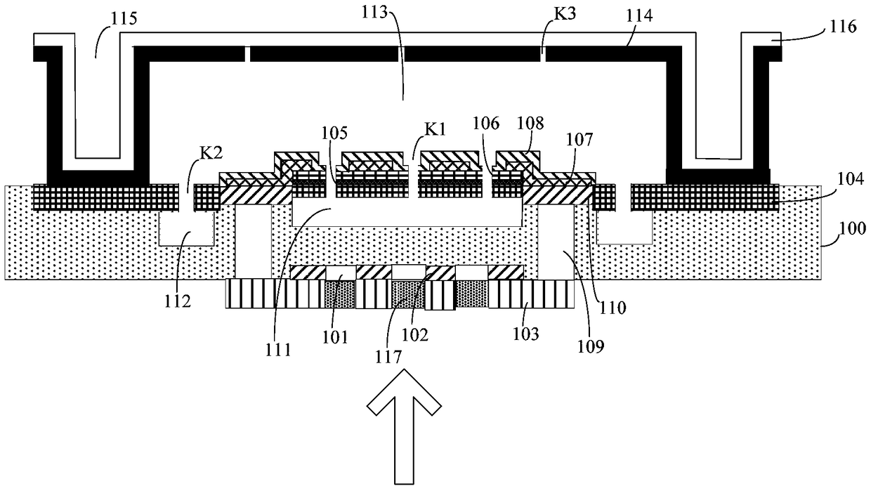
[0047] The pixel structure of the visible-infrared hybrid imaging detector of the present invention includes: a wafer used as a filter layer for filtering out visible light, near-infrared light and mid-infrared light; a visible light sensing area located on the lower surface of the wafer, which includes The visible light sensing part and the first lead-out pole that outputs the electrical signal formed by the visible light sensing part; the external circuit on the lower surface of the wafer located outside the edge of the visible light sensing area, and the infrared...


PUM


Abstract

An image element structure of a visible light and infrared light mixed imaging detector and a fabricating method therefor, comprising: a wafer (100) used as a light filtering layer; a visible light inductive area and an external circuit; a media layer (104); and an infrared light inductive area. The infrared light inductive area comprises: an infrared light inductive component (106); an electrode layer (107); an upper release protection layer (108), wherein a first release hole (K1) is provided at the portion where the bottom of the release protection layer in the electrode layer is in contact with the top of the infrared light inductive component; a first cavity (111) below the first release hole; a plurality of through-holes (109) below the edge of the electrode layer; a second release hole (K2) of the media layer at the outer side of the through-holes; a second cavity below the second release hole; a support component (114) of a third release hole (K3) at the top; a third cavity (113) between the support component and the infrared light inductive area; and a coverage material layer (116).

Description

technical field [0001] The invention relates to the technical field of microelectronics, in particular to a visible-infrared hybrid imaging detector pixel structure and a preparation method thereof. Background technique [0002] With the development of industry and living standards, pure infrared imaging or pure visible light imaging can no longer meet the demand. Imaging technologies with wider wavelength bands have attracted more and more attention, especially imaging technologies that are sensitive to visible light and infrared light at the same time. [0003] However, in existing hybrid imaging devices, lenses are used to form two optical paths to sense and image visible light and infrared light respectively, and finally a computer processing system is used to synthesize them together. Due to the separation of the optical paths, the formed infrared image part and visible light image Some of them have large alignment deviations, which seriously affect the imaging quality....

Claims


Application Information

Patent Timeline
Patent Type & Authority Patents(China)
IPC IPC(8): H01L27/146
CPCH01L27/146
Inventor 康晓旭陈寿面
Owner SHANGHAI INTEGRATED CIRCUIT RES & DEV CENT
Why Eureka
Try Eureka