A kind of gan device and its manufacturing method
A device and nucleation layer technology, used in semiconductor/solid-state device manufacturing, semiconductor devices, electrical components, etc., can solve problems such as large stress, sensor fabrication, cracks, etc., achieve early warning of excessive local electric field, ensure normal operation, process simple effect
- Summary
- Abstract
- Description
- Claims
- Application Information
AI Technical Summary
Problems solved by technology
Method used
Image

Examples
Embodiment Construction
[0027] By providing a GaN device and a manufacturing method thereof, the present invention can effectively manufacture electrodes in the GaN layer, thereby achieving the technical effect of not affecting the working state of the GaN device.
[0028] In order to solve the above-mentioned technical problems, the above-mentioned technical solutions will be described in detail below in conjunction with the accompanying drawings and specific implementation methods.
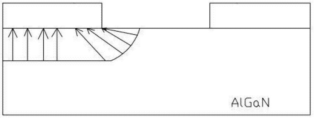
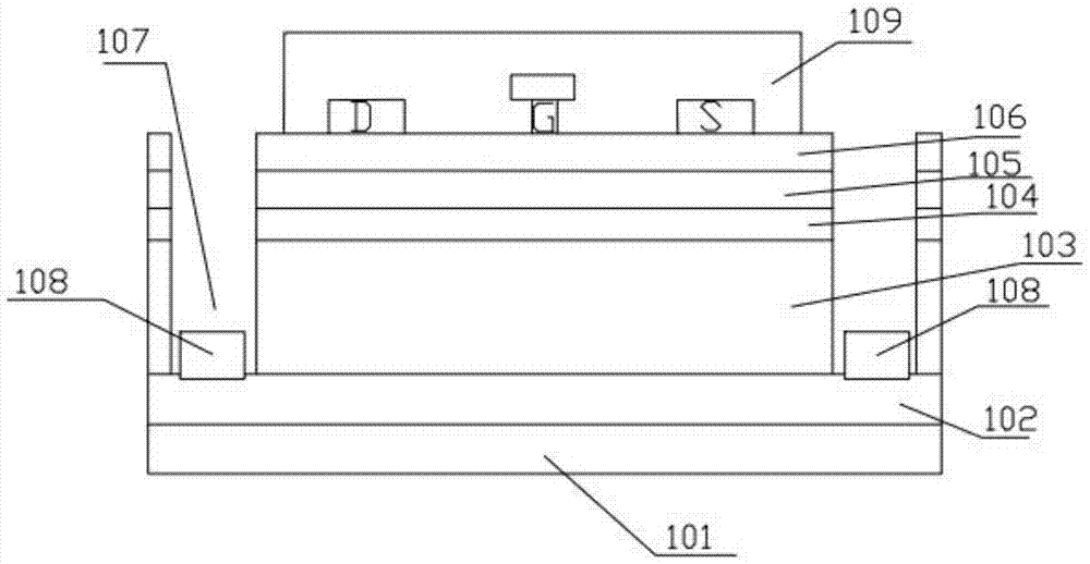
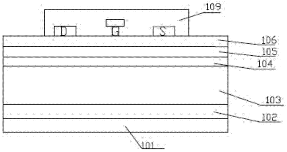
[0029] An embodiment of the present invention provides a GaN device, such as figure 2 As shown, it includes a substrate 101, an AlN nucleation layer 102, a GaN transition layer 103, an AlN isolation layer 104, an AlGaN barrier layer 105, and a GaN cap layer 106 arranged in sequence from bottom to top, and the device on the GaN cap layer 106 The gate G, the source S and the drain D are arranged in a region, and a groove 107 is opened in the detection region on both sides of the device region, and the groove 107 is embe...
PUM
 Abstract
Description
Claims
Application Information
PatSnap Eureka turns technology decisions into work you can execute. Powered by our Innovation Knowledge Graph, it runs expert workflows across engineering, life sciences, materials and intellectual property. Get your review-ready output in minutes.


