Ultra-small ultra-thin high-luminous-efficiency lateral-emission-type high-light white-light LED element

A high-efficiency, LED chip technology, applied in the direction of electrical components, electrical solid-state devices, semiconductor devices, etc., can solve the problems of large size, high-brightness white light cannot solve the problem of heat dissipation, high thermal resistance of PCB, etc., to achieve space saving and good heat dissipation effect , the effect of reducing the size of the product

Inactive Publication Date: 2016-01-27
AMICC OPTO ELECTRONICS TECH
View PDF3 Cites 9 Cited by
  • Summary
  • Abstract
  • Description
  • Claims
  • Application Information

AI Technical Summary

Problems solved by technology

[0004] (2) PCB type: mainly use BT resin as the substrate, the main dimensions are 0603 (1.6*1.1*0.6mm), 0805 (2.0*1.1*0.6mm), 1204 (3.0*1.5*1.0mm), PCB type side Due to the large size of the traditional process and the high thermal resistance of the PCB, the high-brightness white light cannot solve the heat dissipation problem at present

Method used


Image

  • Ultra-small ultra-thin high-luminous-efficiency lateral-emission-type high-light white-light LED element
  • Ultra-small ultra-thin high-luminous-efficiency lateral-emission-type high-light white-light LED element
  • Ultra-small ultra-thin high-luminous-efficiency lateral-emission-type high-light white-light LED element

Examples


Embodiment Construction

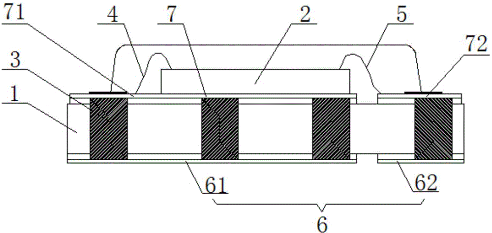
[0029] Such as figure 1 An ultra-small, ultra-thin, high-efficiency side-emitting high-brightness white LED element shown includes a substrate 1 and a light-emitting LED chip 2 , and the light-emitting LED chip 2 is fixed on the substrate 1 . The substrate 1 is provided with a number of via holes penetrating through its upper and lower bottom surfaces, and conductors 3 are filled in the via holes, and the anode of the light-emitting LED chip 2 connects with the anode wire 4 in one of the via holes. The conductor 3 is electrically connected, and the negative electrode of the light-emitting LED chip 2 is electrically connected to the conductor 3 in another via hole through the negative electrode wire 5 . Preferred embodiment: the conductor 3 is a copper pillar or conductive glue.

[0030] The lower bottom surface of the substrate 1 is covered with a first metal conductive layer 6, the metal conductive layer 6 is divided into a positive electrode region 61 and a negative electro...


PUM


Abstract

The invention relates to an ultra-small ultra-thin high-luminous-efficiency lateral-emission-type high-light white-light LED element which comprises a substrate and a light-emitting LED chip. The light-emitting LED chip is fixed on the substrate; the substrate is provided with a plurality of via holes running through the upper and lower surfaces thereof; each via hole is filled with an electric conductor; the positive electrode of the light-emitting LED chip is electrically connected with the electric conductor in one of the via holes through a positive wire; and the negative electrode of the light-emitting LED chip is electrically connected with the electric conductor in another one of the via holes through a negative wire. The provided ultra-small ultra-thin high-luminous-efficiency lateral-emission-type high-light white-light LED element is ultra-thin in thickness and good in heat radiation effect.

Description

technical field [0001] The invention relates to an ultra-small, ultra-thin, high-efficiency side-emitting high-brightness white LED element, in particular to a small side-emitting LED element. Background technique [0002] At present, there are two types of small side-emitting LED indicators on the market: [0003] (1) Bracket type: mainly use PPA resin + copper bracket as the substrate, the main dimensions are 020 (3.8*1.05*0.6mm), 010 (3.8*1.0*0.4mm), 215 (2.8*1.0*0.9mm), 335 (3.8*0.6*1.2mm), its size is relatively large, and the bracket-type side-firing LEDs are mainly concentrated in the 020 and 010 models, but the thinnest thickness is 0.4mm. [0004] (2) PCB type: mainly use BT resin as the substrate, the main dimensions are 0603 (1.6*1.1*0.6mm), 0805 (2.0*1.1*0.6mm), 1204 (3.0*1.5*1.0mm), PCB type side Due to the large size of the traditional process and the high thermal resistance of the PCB, the high-brightness white light cannot solve the heat dissipation problem...

Claims


Application Information

Patent Timeline
Patent Type & Authority Applications(China)
IPC IPC(8): H01L25/075H01L33/48H01L33/62H01L33/64
CPCH01L2224/48091H01L2224/48227H01L2224/48237H01L2924/181H01L2924/00014H01L2924/00012
Inventor 蔡志嘉窦鑫
Owner AMICC OPTO ELECTRONICS TECH
Why Eureka
Try Eureka