Semiconductors lamp

A semiconductor and substrate technology, applied in the field of retrofit lamps with form factors, can solve the problems of limited casting materials and components, expensive casting materials and/or components, and high cost, and achieve simple and compact layout. Effect

Active Publication Date: 2016-02-03
LEDVANCE GMBH
View PDF5 Cites 2 Cited by
  • Summary
  • Abstract
  • Description
  • Claims
  • Application Information

AI Technical Summary

Problems solved by technology

Particularly laborious and costly when sorting to find suitable and compatible materials
The types of casting materials and components that

Method used


Image

  • Semiconductors lamp
  • Semiconductors lamp
  • Semiconductors lamp

Examples


Embodiment Construction

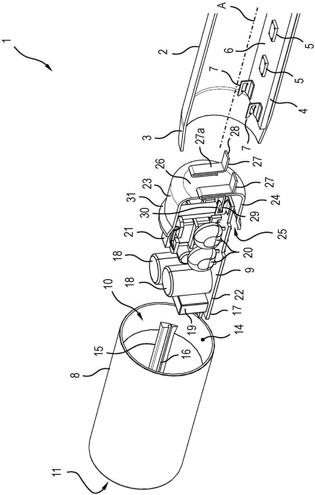
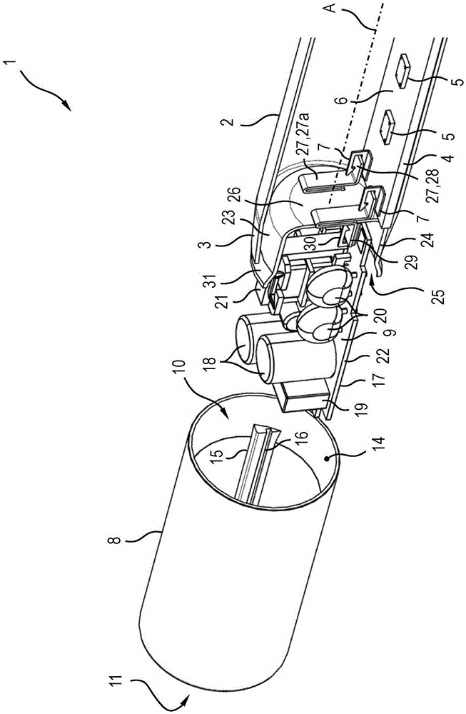
[0040] figure 1 A section through the not yet assembled end-side parts of a semiconductor lighting device, which is designed in the form of an LED retrofit lamp 1 for replacing, for example, a T5 or T8, is shown in a partial sectional view at an oblique angle of view. A type of conventional fluorescent lamp collaborator that replaces linear lamps.

[0041] The LED retrofit lamp 1 has a tubular bulb 2 shown in cutaway with the basic shape of a hollow cylinder, which is made of a light-transmissive (for example transparent or translucent or opaque) material such as glass or synthetic material . The bulb 2 has a constricted end region 3 . This region has an inclination angle relative to the longitudinal axis A of between 5° and 7° in the longitudinal section along the longitudinal axis A of the bulb 2 and thus of the LED retrofit lamp 1 .

[0042] A light source substrate in the form of a strip-shaped printed circuit board 4 , which is equipped with semiconductor light sources...


PUM


Abstract

A semiconductor lamp (1) includes a tubular, at least partially diaphanous bulb shell (2), at least one semiconductor light source (5) disposed in the bulb shell (2), two end covers (8) used for fixing the semiconductor lamp (1) on a frame and a driver (9). The driver is provided with one or more electrical and/or electronic components (18-21), and is at least partially housed in an end cover (8). The components (18-21) of the driver (9) disposed in the end cover (8) are gas-tightly separated from the at least one semiconductor light source (5). The semiconductor lamp is particularly applicable to retrofit, in particular having a shape factor of linear fluorescent lamps.

Description

technical field [0001] The invention relates to a semiconductor lamp with: a tubular, at least partially light-transmitting bulb; at least one semiconductor light source arranged in the bulb; two end caps for fixing the semiconductor lamp on a socket; and A driver having one or more electrical and / or electronic components mounted at least partially in the end cap. The present invention is particularly useful for retrofit lamps, especially retrofit lamps having the form factor of a linear fluorescent lamp. Background technique [0002] A problem with LED lamps of the type concerned with light-emitting diodes ("LEDs") as semiconductor light sources is that electrical and / or electronic components or parts are often embedded in organic casting materials (so-called "potting"). Encapsulation" material), thereby improving thermal conductivity. The electrical and / or electronic components themselves can also have a high proportion of organic materials, such as capacitors or printed...

Claims


Application Information

Patent Timeline
IPC IPC(8): F21K9/27F21K9/272F21V3/04F21V23/00F21V23/06F21Y115/10F21Y103/10
CPCF21V3/02F21V3/04F21V23/003F21V23/06F21K9/278F21V15/015F21V23/006F21V23/007F21V31/04
Inventor 托马斯·比特曼约翰·迈尔
Owner LEDVANCE GMBH
Why Eureka
Try Eureka