
Pixel recession compensation circuit of silicon-based organic light emitting micro-display

A technology of micro-display and compensation circuit, which is applied in the direction of static indicators, instruments, etc., can solve the problems of poor luminous consistency, bright luminous light, and dark luminous light, etc., and achieve the effect of good luminous consistency

Inactive Publication Date: 2016-02-03
SHANGHAI UNIV
View PDF6 Cites 10 Cited by
  • Summary
  • Abstract
  • Description
  • Claims
  • Application Information

AI Technical Summary

Problems solved by technology

When OLED displays high-contrast and high-brightness displays for a long time, the OLED pixels decay inconsistently, resulting in poor luminous consistency. When the screen is refreshed, blurred afterimages will be observed. The place where the original luminous brightness is dark decays slowly, and the luminous light will be brighter. , and the place where the original luminous brightness is high decays faster, and the luminous light will be dim

Method used


Image

  • Pixel recession compensation circuit of silicon-based organic light emitting micro-display
  • Pixel recession compensation circuit of silicon-based organic light emitting micro-display
  • Pixel recession compensation circuit of silicon-based organic light emitting micro-display

Examples


Embodiment 1

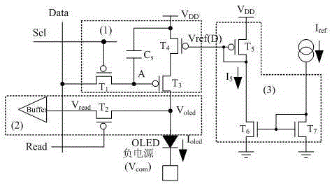
[0041] See figure 1 , A silicon-based organic light emitting microdisplay pixel degradation compensation circuit, which is composed of a pixel unit circuit (1) connected to an anode voltage readout circuit (2) of an organic light emitting diode and a reference current generating circuit (3).

[0042] The pixel unit circuit (1) includes a first switching transistor T1, a third switching transistor T3, a storage capacitor Cs, and a driving transistor T4;

[0043] The first switching transistor T1: the drain is connected to the array driving signal Data, the gate is connected to the row driving signal Sel, the source is connected to the gate of the third switching transistor T3, and connected to the power supply Vdd via the storage capacitor Cs; the first switching transistor T1 When the row drive signal Sel is valid, write the column drive signal Data into the storage capacitor Cs;

[0044] The third switching transistor T3: the drain is connected to the anode of the organic light emit...

Embodiment 2

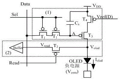
[0056] This embodiment is basically the same as the first embodiment, and the special features are as follows:

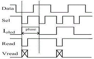
[0057] In the silicon-based organic light-emitting microdisplay pixel degradation compensation circuit, the pixel unit circuit can generate pulse width modulation waveforms, and the pixel unit circuit can be controlled by digital driving; the operating current of the silicon-based organic light-emitting diode can be from 1nA to 1uA, depending on the difference The cell size of the OLED, by adjusting the value of Iref, while the voltage at the two ends of the OLED is constantly changing, to ensure that the OLED can work at the appropriate brightness. Vref can be obtained through a fixed voltage source, an active current mirror, and a self-biased low voltage cascode current mirror.

[0058] The pixel degradation compensation circuit of the silicon-based organic light-emitting microdisplay is characterized in that the pixel driving unit can transmit the column driving signa...


PUM


Abstract

The invention relates to a pixel recession compensation circuit of a silicon-based organic light emitting micro-display. The compensation circuit is formed by a pixel unit circuit, an anode pressure reading-out circuit and a reference current generating circuit. The pixel unit circuit comprises three switch transistors, a driving transistor, a storage capacitor and an organic light emitting diode. The grid electrode of the first switch transistor is connected with a line driving signal, the drain electrode is connected with a row driving signal, and the source electrode is connected with the grid electrode of the third switch transistor. When the first switch transistor carries out line gating, the line driving signal is written into the storage capacitor so as to control the state of the third switch transistor. The drain electrode of the third switch capacitor is connected with the anode of the organic light emitting diode and the source electrode is connected with the drain electrode of the driving transistor. The source electrode of the driving transistor is connected with a positive power supply and the grid electrode is connected with reference current of the reference current generating circuit. The reading-out circuit is formed by the second switch transistor, the grid electrode of the reading-out circuit is connected with a reading-out signal and the source electrode is connected with the anode of the organic light emitting diode. When the reading-out signal is valid, the drain electrode of the second switch transistor outputs anode voltage.

Description

Technical field [0001] The invention relates to a pixel degradation compensation circuit of a silicon-based organic light-emitting microdisplay. Background technique [0002] Silicon-based organic light-emitting diodes (OLED-on-Silicon, OrganicLightEmittingDiodeonSilicon) are a combination of organic light-emitting diodes and monocrystalline silicon integrated circuits. CMOS process has the characteristics of low cost and small size, which is the cornerstone of the integrated circuit industry; OLED has the advantages of low power consumption, self-luminous, wide viewing angle, low cost, good temperature adaptability, and fast response speed. The advantages of the combination of the two make silicon-based organic light-emitting diodes a new type of display technology that has attracted much attention. [0003] Generally, a display with a screen diagonal of less than 3.3 cm is defined as a micro display. The size of the micro display itself is small, but it can achieve a super larg...

Claims


Application Information

Patent Timeline
Patent Type & Authority Applications(China)
IPC IPC(8): G09G3/3233
Inventor 季渊王成冉峰徐洪光沈伟星
Owner SHANGHAI UNIV
Learn More