Efficient heat dissipation substrate for optoelectronic devices

A technology for optoelectronic devices and heat-dissipating substrates, which is used in electrical solid-state devices, electrical components, and semiconductor devices. Thermal conductivity, the effect of improving the overall heat dissipation capacity

Active Publication Date: 2018-03-02
SHANGHAI UNIV
View PDF3 Cites 1 Cited by
  • Summary
  • Abstract
  • Description
  • Claims
  • Application Information

AI Technical Summary

Problems solved by technology

The low thermal conductivity of FR4 cannot meet the heat dissipation requirements of the device, and the ceramic substrate is difficult to form, it is difficult to obtain a large-area plate, and it is difficult to reduce the cost, which cannot meet large-scale use. Therefore, the current development of optoelectronic device packaging substrates focuses on MCPCB substrates
The choice of insulating layer material on the MCPCB substrate will also affect the overall heat dissipation performance. Generally, the insulating layer on the MCPCB is mostly an epoxy layer, which can meet the insulation requirements, but the thermal conductivity is poor, which greatly affects the overall heat dissipation of the device.
The MCPCB substrate generally uses aluminum as the main metal substrate, and its blackness is low, which cannot effectively use the heat radiation channel to improve the heat dissipation performance of the MCPCB

Method used


Image

  • Efficient heat dissipation substrate for optoelectronic devices
  • Efficient heat dissipation substrate for optoelectronic devices
  • Efficient heat dissipation substrate for optoelectronic devices

Examples


Embodiment 1

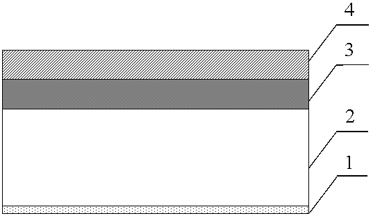
[0024] In this example, see figure 1 , a high-efficiency heat dissipation substrate for optoelectronic devices, heat dissipation is carried out from its conductive layer 4, and a composite heat dissipation substrate is formed by stacking a heat-conducting insulating layer 3, a metal substrate 2 and a carbon-based material coating 1 in sequence, wherein the heat-conducting insulating layer 3 The surface on the other side of the carbon-based material coating 1 is closely combined with the conductive layer 4 of the optoelectronic device, and the exposed surface on the other side of the carbon-based material coating 1 forms the external heat dissipation surface of the composite heat dissipation substrate, which passes the heat generated by the optoelectronic device during operation through the conductive layer 4, Then it is led out through the heat-conducting insulating layer 3, the metal substrate 2 and the carbon-based material coating 1 in order to dissipate heat.

[0025] In t...

Embodiment 2

[0028] This embodiment is basically the same as Embodiment 1, especially in that:

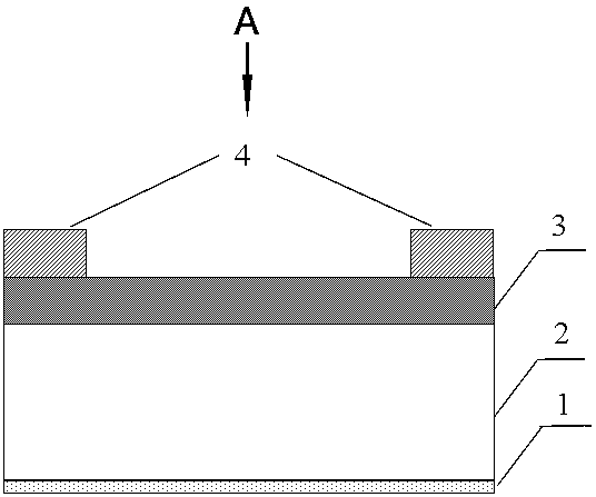
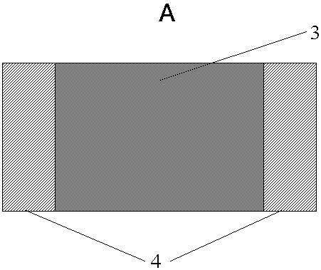
[0029] In this example, see figure 2 and image 3 A high-efficiency heat dissipation substrate for optoelectronic devices includes a metal substrate 2, a carbon-based material coating 1 located on the lower surface of the metal substrate, a thermally conductive insulating layer 3 located on the upper surface of the metal substrate, and a conductive layer 4 located on the upper surface of the thermally conductive insulating layer. The metal substrate 2 is made of copper and has a thickness of 1.5 mm. The graphene / carbon nanotube composite coating on the lower surface of the metal substrate 2 has a thickness of 1 nm. A thermally conductive insulating layer 3 is covered on the surface of the metal substrate 2, and the material of the thermally conductive insulating layer 3 is AlN doped with element zirconium, with a thickness of 5um and a thermal conductivity of 20 W / (m·K). There is a conducti...


PUM

PropertyMeasurementUnit
thicknessaaaaaaaaaa
thicknessaaaaaaaaaa
thicknessaaaaaaaaaa

Abstract

The invention discloses a high-efficiency heat dissipation substrate for optoelectronic devices. Heat dissipation is carried out from its conductive layer, and a composite heat dissipation substrate is formed by sequentially laminating and combining a heat conduction insulating layer, a metal substrate and a carbon-based material coating, wherein another part of the heat conduction insulation layer One side of the surface is closely combined with the conductive layer of the optoelectronic device, and the exposed surface of the other side of the carbon-based material coating forms the external heat dissipation surface of the composite heat dissipation substrate. Layers, metal substrates and carbon-based material coatings are exported to dissipate heat. The invention improves the dielectric constant, antistatic ability and heat dissipation ability of the substrate by coating a layer of thermally conductive and insulating ceramic coating on the upper surface of the high thermal conductive metal substrate as an insulating layer; the lower surface of the metal substrate is coated with a layer of carbon with good thermal conductivity. The base material coating has high thermal conductivity and thermal radiation coefficient, which can further improve the overall heat dissipation performance of the substrate.

Description

technical field [0001] The invention relates to a photoelectric device, in particular to a heat dissipation part of the photoelectric device, which is applied in the technical field of photoelectric device heat dissipation. Background technique [0002] In recent years, with the rapid development of intelligent and miniaturized electronic products, the power density of electronic components has increased significantly while the physical size has become smaller and smaller, and the heat flux has also increased. The corresponding rise in junction temperature will inevitably affect The performance of electronic components requires more efficient thermal control. Therefore, effectively solving the heat dissipation problem of electronic components has become a key technology in the manufacture of electronic components and electronic equipment. [0003] As one of the typical electronic products, the thermal management of optoelectronic devices has also become one of the important...

Claims


Application Information

Patent Timeline
Patent Type & Authority Patents(China)
IPC IPC(8): H01L23/373H01L23/14
Inventor 杨连乔刘亚男殷录桥张建华
Owner SHANGHAI UNIV
Why Eureka
Try Eureka