Metal layer-insulator layer-metal layer capacitor and manufacturing method thereof
What is AI technical title?
AI technical title is built by Patsnap AI team. It summarizes the technical point description of the patent document.
A manufacturing method and metal layer technology, applied in the direction of electrical solid-state devices, semiconductor/solid-state device manufacturing, circuits, etc., can solve problems such as the inability to meet the needs of large-capacity integrated circuits, achieve large capacitance values, and increase capacitance density.
Active Publication Date: 2019-12-17
GALAXYCORE SHANGHAI
View PDF7 Cites 0 Cited by
Summary
Abstract
Description
Claims
Application Information
AI Technical Summary
This helps you quickly interpret patents by identifying the three key elements:
Problems solved by technology
Method used
Benefits of technology
Problems solved by technology
For MIM capacitors with a planar structure, the capacitance density can reach up to 4 - 6 fF / μm 2 , but in practical applications, it is still far from meeting the needs of large-capacitance integrated circuits such as LCD drive circuits and RFCMOS circuits.
Method used
Image
Click on the blue label to locate the original text in one second.
Reading with bidirectional positioning of images and text.
Examples
Embodiment 1
[0039] Figure 1-Figure 10 It is a process schematic diagram of the manufacturing method of the metal layer-insulation layer-metal layer capacitor according to Embodiment 1 of the present invention.
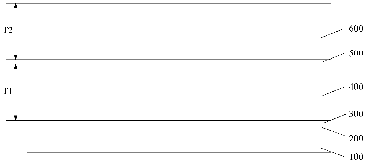
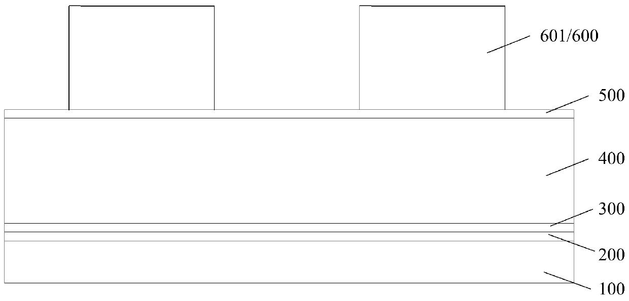
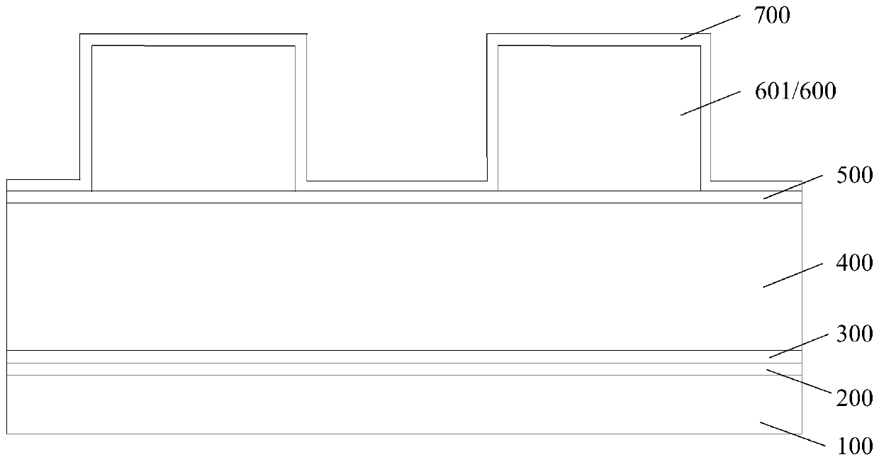
[0040] see figure 1 , providing a first metal layer 100, defining a non-capacitive area and a capacitive area on the first metal layer 100, figure 1 Only the structure of the capacitive region is shown here, and the structure of the non-capacitive region is not shown.
[0041] In the capacitor area, the first dielectric layer 400 , the third barrier layer 500 , and the second dielectric layer 600 are sequentially formed on the surface of the first metal layer 100 . Wherein, the thickness T1T1 of the first dielectric layer 400 is 50 nm-5 μm, and the thickness T2 of the second dielectric layer 600 is 50 nm-5 μm.
[0042] In addition, the adhesion layer 200 and the second barrier layer 300 are preferably sequentially formed on the first metal layer 100 before the step of formin...
Embodiment 2
[0069] Figure 11-Figure 20 It is a process schematic diagram of the manufacturing method of the metal layer-insulation layer-metal layer capacitor according to Embodiment 2 of the present invention.
[0070] see Figure 11 , providing a first metal layer 2100, defining a non-capacitive area and a capacitive area on the first metal layer 2100, Figure 11 Only the structure of the capacitive region is shown here, and the structure of the non-capacitive region is not shown.
[0071] In the capacitor area, a first dielectric layer 2400 is formed on the surface of the first metal layer 2100 . Wherein, the total thickness of the first dielectric layer 2400 is T0. In addition, preferably before the step of forming the first dielectric layer 2400 , the adhesion layer 2200 and the second barrier layer 2300 are sequentially formed on the first metal layer 2100 . Wherein, the adhesion layer 2200 is usually a TiN layer, and the second barrier layer 2300 can be any one or a combinatio...
PUM
Property
Measurement
Unit
thickness
aaaaa
aaaaa
thickness
aaaaa
aaaaa
height
aaaaa
aaaaa
Abstract
The invention provides a metal layer-insulating layer-metal layer capacitor and belongs to the field of in-chip capacitors of integrated circuits. The metal layer-insulating layer-metal layer capacitor comprises a first metal layer; a non-capacitor region and a capacitor region are defined on the first metal layer; a plurality of cofferdam side walls which are located in the capacitor region are arranged on the surface of the first metal layer; the cofferdam side wall includes a first dielectric layer located at the bottom and a first barrier layer located on the first dielectric layer; grooves are correspondingly formed in the cofferdam side walls; a capacitor lower pole plate, a capacitor dielectric layer and a capacitor upper pole plate are sequentially arranged at the surfaces of the cofferdam side walls and the grooves; a conducting plug layer is arranged on the capacitor upper pole plate; and a second metal layer is arranged on the conducting plug layer. According to the MIM (metal layer-insulating layer-metal layer) capacitor of the invention, a stereoscopic structure is adopted, and therefore, effective electrode areas corresponding to the capacitor upper pole plate and the capacitor lower pole plate are increased, and capacitance density can be increased, and thus, a larger capacitance value can be obtained based on a limited chip area, and requirements of large-capacitance integrated circuits such as an LCD driving circuit and an RFCMOS circuit can be satisfied. The metal layer-insulating layer-metal layer capacitor can be used as in-chip capacitors of integrated circuits.
Description
technical field [0001] The invention relates to the field of integrated circuits, in particular to a metal layer-insulation layer-metal layer capacitor and a manufacturing method thereof. Background technique [0002] The application of capacitors is always a lever in integrated circuit design. Designers hope to use capacitors with as large a capacitance as possible, but large capacitances often lead to increased chip area and increased manufacturing costs. How to increase the capacitance value per unit chip area (that is, capacitance density) has always been a challenge in the field of integrated circuits. [0003] Existing capacitors can be roughly divided into front-end capacitors and back-end capacitors, front-end capacitors such as MOS capacitors, PN junction capacitors, back-end capacitors such as MIM (metal layer-insulation layer-metal layer) capacitors, MOM (metal layer- oxide layer - metal layer) capacitor. Among them, MIM capacitors can provide better frequency a...
Claims
Application Information
Patent Timeline
Application Date:The date an application was filed.
Publication Date:The date a patent or application was officially published.
First Publication Date:The earliest publication date of a patent with the same application number.
Issue Date:Publication date of the patent grant document.
PCT Entry Date:The Entry date of PCT National Phase.
Estimated Expiry Date:The statutory expiry date of a patent right according to the Patent Law, and it is the longest term of protection that the patent right can achieve without the termination of the patent right due to other reasons(Term extension factor has been taken into account ).
Invalid Date:Actual expiry date is based on effective date or publication date of legal transaction data of invalid patent.

