Manufacturing method of capacitor

A manufacturing method and technology of capacitors, which can be used in semiconductor/solid-state device manufacturing, circuits, electrical components, etc., and can solve problems such as large leakage current and reduced linearity.

Inactive Publication Date: 2006-08-16
TAIWAN SEMICON MFG CO LTD
View PDF0 Cites 0 Cited by
  • Summary
  • Abstract
  • Description
  • Claims
  • Application Information

AI Technical Summary

Problems solved by technology

One of the ways to increase the capacitance density is to reduce the thickness of the dielectric layer, but at the cost of reduced linearity and larger leakage current due to larger operating electric field
Another way to increase capacitance density is to use high dielectric constant (High-k) materials, such as tantalum pentoxide. However, electrode materials with special structures must be used in complex process integration.

Method used


Image

  • Manufacturing method of capacitor
  • Manufacturing method of capacitor
  • Manufacturing method of capacitor

Examples


Embodiment Construction

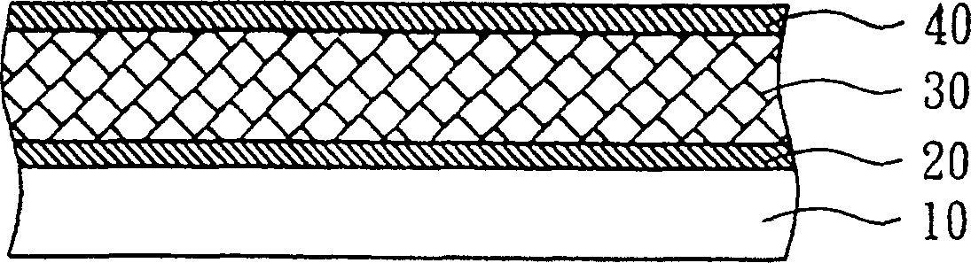
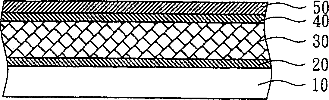
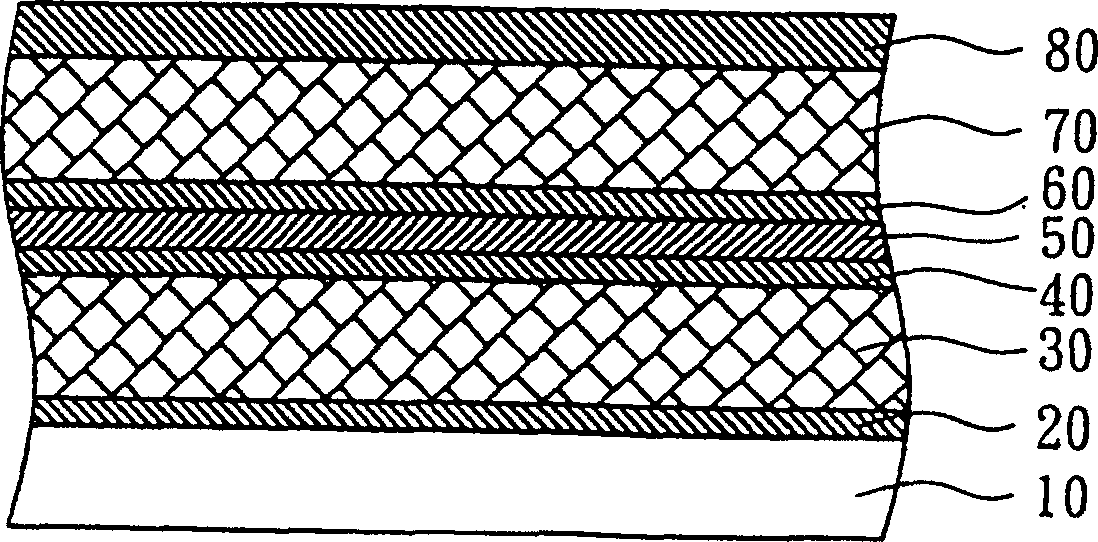
[0058] The invention relates to a manufacturing method of a three-dimensional MIM capacitor. Figure 2A to Figure 2N It is a cross-sectional view of the structure of the manufacturing method of the three-dimensional MIM capacitor according to the first preferred embodiment of the present invention. Such as Figure 2A Firstly, a substrate 210 is provided, wherein some CMOS devices (not shown) have been pre-formed on the substrate 210 . Next, an adhesive layer 220 is formed on the base material 210, wherein the material of the adhesive layer 220 can be titanium nitride, and the thickness of the adhesive layer 220 can be about 250 Å, for example. The purpose of this adhesive layer 220 is to strengthen the adhesion between the metal layer and the substrate 210 in the subsequent process and as a barrier layer, and the purpose of other adhesive layers in this specification is to strengthen the metal layer and other layers. Adhesion as well as acting as a barrier layer. Next, a me...


PUM


Abstract

A process for preparing the metal-insulator-metal (MIM) capacitor features that a 3D cup-shaped spacer structure is formed on the surface of a metallic plane to increase the electrode area of capacitor. Its preparing process is fully compatible with that of CMOS transistor, and can be used for the mixed-signal or RF signal on chip.

Description

technical field [0001] The present invention relates to a method for manufacturing a capacitor, in particular to a method for manufacturing a metal-insulator-metal (Metal-Insulator-Metal; MIM) capacitor used in integrated circuits. Background technique [0002] In today's Very Large Scale Integration (VLSI), a capacitor is one of the commonly used passive components. Capacitors are often integrated in active components such as bipolar transistors or complementary metal oxide semiconductor (Complementary Metal Oxide Semiconductor; CMOS) transistors. These capacitors are usually in the form of polysilicon-insulator-polysilicon (Polysilicon-Insulator-Polysilicon; PIP), metal-insulator-silicon (Metal-Insulator-Silicon; MIS), or metal-insulator-metal. Based on the compatibility with the process and the simplicity of the process, these different forms of capacitors are all planar. [0003] For mixed-signal (Mixed-signal) or radio frequency (Radio Frequency; RF) applications, MIM...

Claims


Application Information

Patent Timeline
Patent Type & Authority Patents(China)
IPC IPC(8): H01L21/70
Inventor 林大成季明华
Owner TAIWAN SEMICON MFG CO LTD
Why Eureka
Try Eureka