Check patentability & draft patents in minutes with Patsnap Eureka AI!

Structure of a CMOS image sensor and preparation method thereof

An image sensor and silicide technology, applied in radiation control devices and other directions, can solve problems such as light source loss, reduce the loss of reflected light, improve product yield, and increase intensity.

Active Publication Date: 2019-02-22
SHANGHAI HUALI MICROELECTRONICS CORP
View PDF3 Cites 0 Cited by
  • Summary
  • Abstract
  • Description
  • Claims
  • Application Information

AI Technical Summary

Problems solved by technology

Although this technology can reduce the light source loss caused by the refraction of light at the interface of the dielectric material in the back stage, due to the requirements of the production process, a thin film 5 must be reserved on the photodiode 4 as a stop layer for deep groove etching to protect the photodiode 4. surface, the improper thickness of the film 5 will still lead to loss of light source

Method used


Image

  • Structure of a CMOS image sensor and preparation method thereof
  • Structure of a CMOS image sensor and preparation method thereof
  • Structure of a CMOS image sensor and preparation method thereof

Examples


preparation example Construction

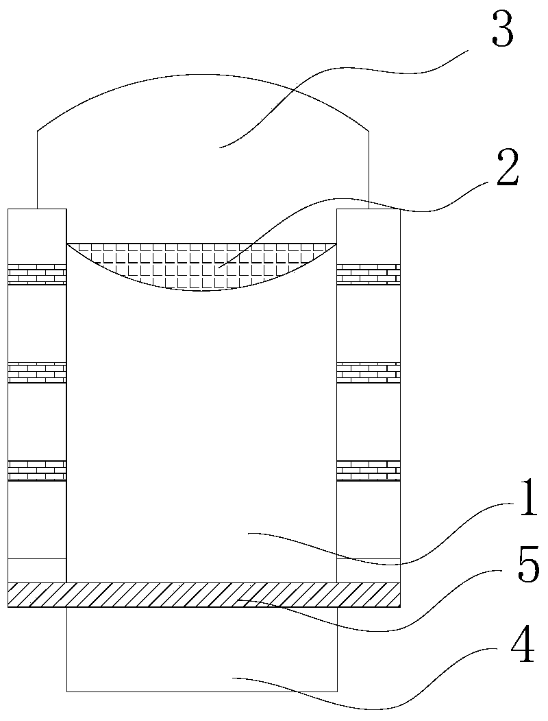
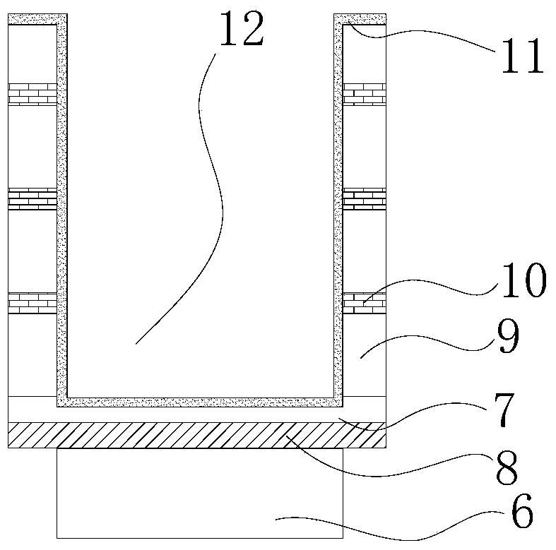
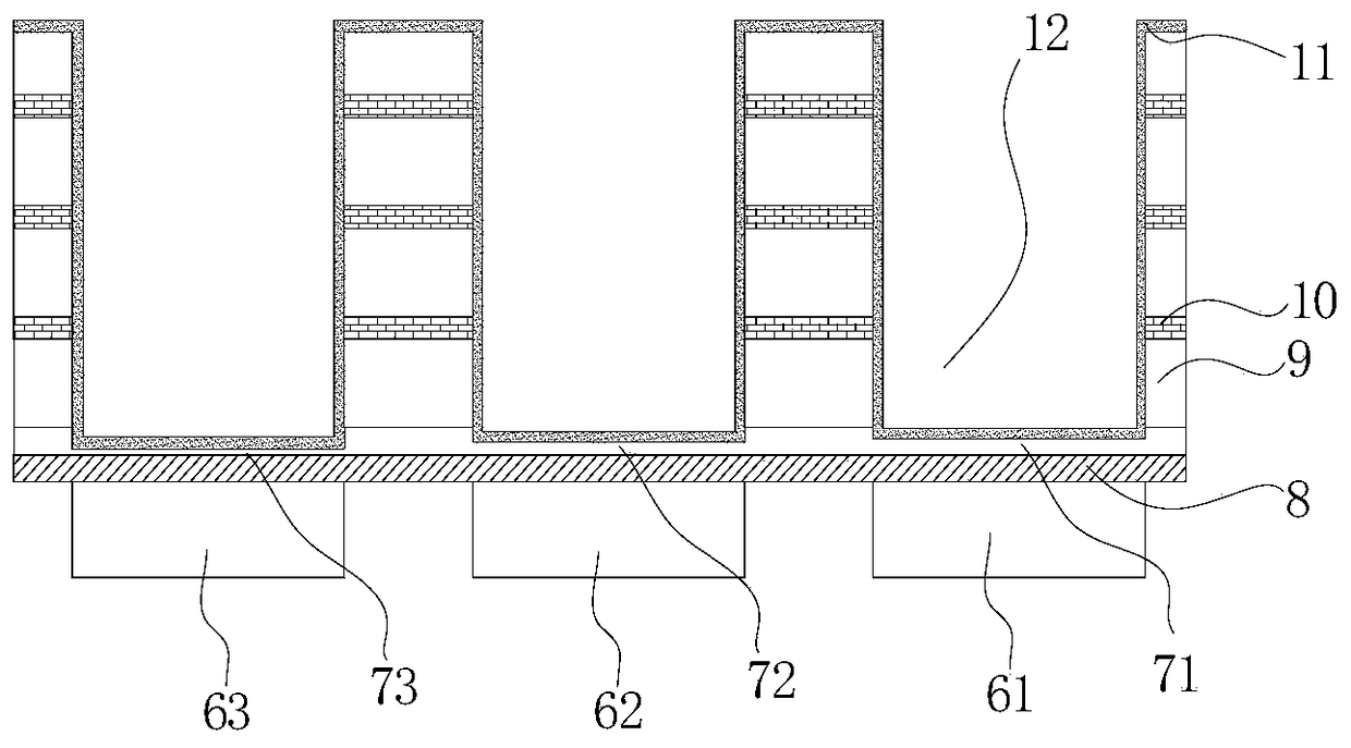
[0037] A method for preparing a CMOS image sensor, characterized in that the method includes providing the photodiode region, and disposing the contact etching barrier layer on the photodiode region;

[0038] Depositing a silicide mask layer on the upper end of the contact etching barrier layer, wherein the total thickness of the silicide mask and the contact etching barrier layer is controlled to be greater than 1 / 4 of the wavelength of the incident light source;

[0039] Etching part of the silicide mask layer, wherein the total thickness of the etched silicide mask and the contact etching barrier layer is less than 1 / 4 of the wavelength of the incident light source;

[0040] depositing the dielectric layer on the surface of the etched silicide mask layer, and using the silicide mask as a stop layer to etch the dielectric layer to form the optical channel deep groove;

[0041] Deposit and form the protective layer film on the entire product surface after etching, wherein the...


PUM


Abstract

The invention relates to the field of semiconductor yield increase, and especially relates to a CMOS image sensor structure and a preparation method thereof. The film thickness is controlled in the making process based on the interference principle of light. Therefore, the loss of reflected light is reduced, and the intensity of transmitted light is increased, which is of great help to the increase of product yield.

Description

technical field [0001] The invention relates to the field of semiconductor yield improvement, in particular to a structure of a CMOS image sensor and a preparation method thereof. Background technique [0002] The manufacturing of the semiconductor industry is changing with each passing day, and the manufacturing process of products is becoming more and more refined. Various defects will kill the yield of products, and improving various factors that cause defects has become an important means to improve the yield of semiconductors. [0003] Such as figure 1 As shown, for the front-illuminated CMOS (Complementary Metal Oxide Semiconductor, CMOS for short) image sensor, the current mainstream method in the industry is to form a deep groove 1 by etching after the passivation layer is completed, and then The resin material is filled in the groove for planarization, and then the filter 2 and the microlens 3 are manufactured to form a complete image sensor. Although this techno...

Claims


Application Information

Patent Timeline
Patent Type & Authority Patents(China)
IPC IPC(8): H01L27/146
Inventor 张武志
Owner SHANGHAI HUALI MICROELECTRONICS CORP
Features
  • R&D
  • Intellectual Property
  • Life Sciences
  • Materials
  • Tech Scout
  • Unparalleled Data Quality
  • Higher Quality Content
  • 60% Fewer Hallucinations
Learn More