A kind of manufacturing method of light-emitting diode with high spreading effect

A technology of light-emitting diodes and manufacturing methods, which is applied in the direction of electrical components, circuits, semiconductor devices, etc., can solve the problems of increasing the light-blocking area of ​​electrodes, and achieve the effect of increasing the external quantum effect

Active Publication Date: 2018-01-16
江西乾照光电有限公司
View PDF4 Cites 0 Cited by
  • Summary
  • Abstract
  • Description
  • Claims
  • Application Information

AI Technical Summary

Problems solved by technology

However, the use of P-type extended electrodes significantly increases the light-blocking area of ​​the electrode; increasing the doping concentration of N-type will increase the effect of N-type current expansion to the limit, and will encounter bottlenecks when applied to large-area chips.

Method used


Image

  • A kind of manufacturing method of light-emitting diode with high spreading effect
  • A kind of manufacturing method of light-emitting diode with high spreading effect

Examples


Embodiment Construction

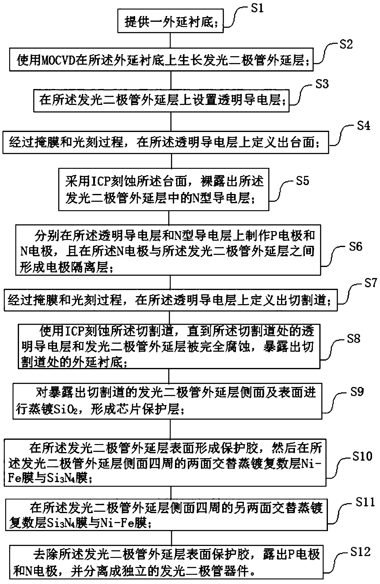
[0036] In order to make the technical problems, technical solutions and beneficial effects to be solved by the present invention clearer and clearer, the present invention will be further described in detail below in conjunction with the accompanying drawings and embodiments. It should be understood that the specific embodiments described here are only used to explain the present invention, not to limit the present invention.

[0037] Such as figure 1 As shown, the present invention provides a method for manufacturing a light-emitting diode with high spreading effect, comprising the following steps:

[0038] S1: providing an epitaxial substrate;

[0039] S2: using MOCVD (metal organic compound chemical vapor deposition) to grow a light emitting diode epitaxial layer on the epitaxial substrate;

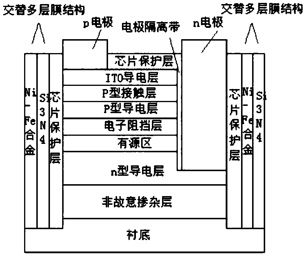
[0040] S3: disposing an ITO transparent conductive layer on the epitaxial layer of the light emitting diode;

[0041] S4: Defining a mesa on the transparent conductive layer through...


PUM

PropertyMeasurementUnit
thicknessaaaaaaaaaa
thicknessaaaaaaaaaa
thicknessaaaaaaaaaa

Abstract

The present invention discloses a manufacture method of a light emitting diode having a high extension effect. The manufacture method comprises the following steps: providing an epitaxial substrate; growing the epitaxial layer of the light emitting diode through adoption of MOCVD; forming protection glue at the surface of the epitaxial layer of the light emitting diode, and performing alternate vacuum evaporation of a plurality of layers of Ni-Fe alloy membranes and Si3N4 membranes at two of four side faces of the epitaxial layer of the light emitting diode; performing alternate vacuum evaporation of a plurality of layers of Si3N4 membranes and Ni-Fe alloy membranes at the other two of four side faces of the epitaxial layer of the light emitting diode; and removing the protection glue at the surface of the epitaxial layer of the light emitting diode, exposing a p electrode and a n electrode, and forming an independent light emitting diode device through separation of epitaxial wafers. According to the invention, N-type and P-type current expansion of a light emitting diode is effectively enhanced without increasing the light blocking area of electrodes, and the N-type current expansion effect of a large-size chip is improved.

Description

technical field [0001] The invention relates to the technical field of light-emitting diodes, and in particular provides a method for manufacturing a light-emitting diode with high spreading effect. Background technique [0002] In recent years, light-emitting diodes have developed rapidly, which is closely related to the development of semiconductor optoelectronic technology and new lighting source technology. With the continuous expansion of LED application fields, people have put forward higher and higher requirements for the performance of LED chips. Therefore, it is necessary to continuously improve the external quantum efficiency of LEDs. [0003] Enhancing the current spreading effect of light-emitting diodes is an important way to improve the external quantum efficiency of LEDs. Currently commonly used methods are: P-type by using P-type extended electrodes, N-type by increasing the doping concentration of N-type and so on. However, the use of P-type extended elec...

Claims


Application Information

Patent Timeline
Patent Type & Authority Patents(China)
IPC IPC(8): H01L33/00H01L33/14
CPCH01L33/005H01L33/14
Inventor 林志伟陈凯轩张永卓祥景姜伟方天足陈亮
Owner 江西乾照光电有限公司
Why Eureka
Try Eureka