Mis-structured UV LED based on localized surface plasmon enhancement and its preparation method

A technology of localized surface plasmon and MIS structure, applied in electrical components, semiconductor devices, circuits, etc., can solve the problems of weak luminous intensity and low internal quantum efficiency of devices, and achieve improved internal quantum efficiency, simple preparation process, enhanced The effect of luminous intensity

Active Publication Date: 2020-05-22
XIAMEN UNIV
View PDF5 Cites 0 Cited by
  • Summary
  • Abstract
  • Description
  • Claims
  • Application Information

AI Technical Summary

Problems solved by technology

[0003] However, due to the lack of quantum wells in MIS-structured UV LEDs, the internal quantum efficiency is low and the luminous intensity of the device is weak.

Method used


Image

  • Mis-structured UV LED based on localized surface plasmon enhancement and its preparation method
  • Mis-structured UV LED based on localized surface plasmon enhancement and its preparation method

Examples


Embodiment Construction

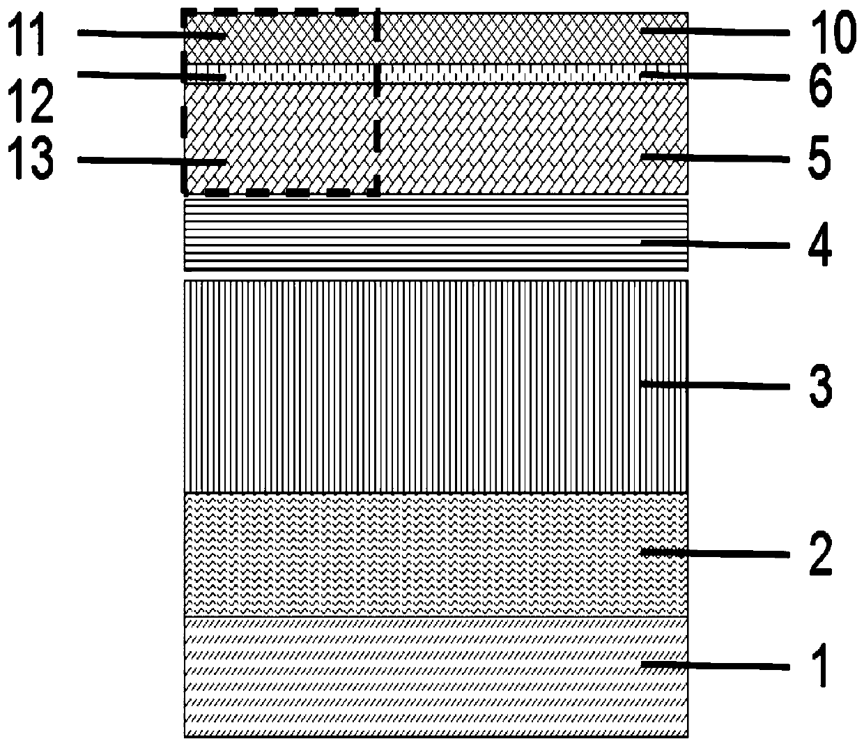
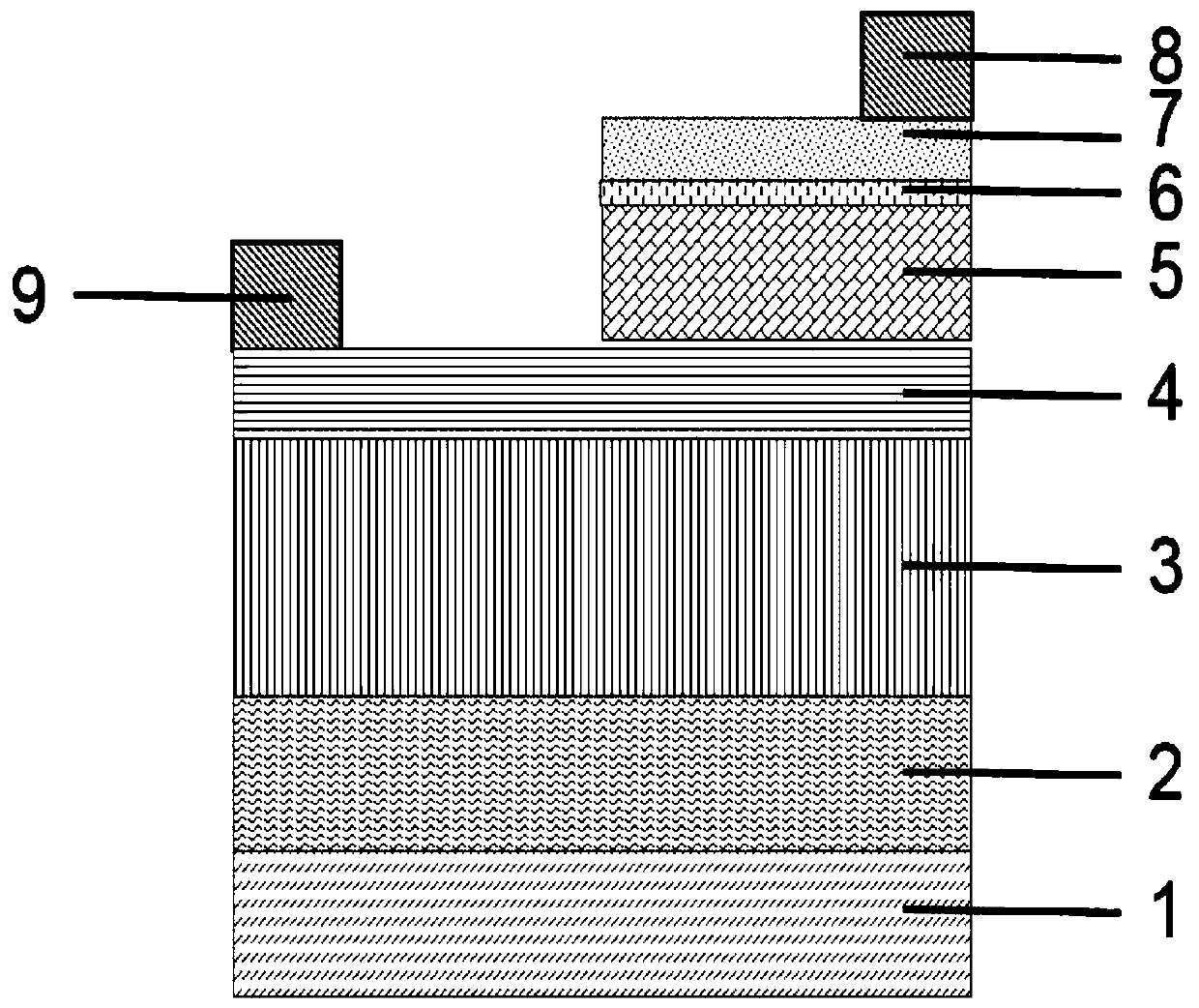
[0032] The present invention will be further described below through specific embodiments. The drawings of the present invention are only schematic diagrams for easier understanding of the present invention, and their specific proportions can be adjusted according to design requirements. The upper and lower relationship of the relative components in the figures described herein should be understood by those skilled in the art to refer to the relative positions of the components. Correspondingly, the upper side of the component is the front and the lower side is the back for easy understanding, so all The same components can be turned over to present, all of which should belong to the scope disclosed in this specification.

[0033] In order to solve the problems of complex process and low internal quantum efficiency in the existing ultraviolet LED technology field, the present invention provides a MIS structure ultraviolet LED based on local surface plasmon enhancement and its ...


PUM

PropertyMeasurementUnit
thicknessaaaaaaaaaa
thicknessaaaaaaaaaa
diameteraaaaaaaaaa

Abstract

The invention relates to an MIS structured ultraviolet LED based on local surface plasmon enhancement and a preparation method thereof. According to the invention, silver metal nanoparticles are introduced into the MIS structured ultraviolet LED to form a local surface plasmon; the MIS structured LED adopts a graphene film to serve as a conductive layer so as to enhance the current expansibility and improve the ultraviolet light emitting rate of the device; and the metal nanoparticles are arranged on the graphene layer, and emitted photons are enabled to have resonance coupling with the metalnanoparticles by using the local surface plasmon enhancement effect, so that the internal quantum efficiency of the device is improved, and the light emitting intensity of the device is enhanced. TheMIS structured ultraviolet LED based on the local surface plasmon enhancement provided by the invention has the advantages of simple structure, simple and convenient preparation and easy production.

Description

technical field [0001] The invention belongs to the technical field of semiconductor optoelectronic devices, and in particular relates to a MIS structure ultraviolet LED based on localized surface plasmon enhancement and a preparation method thereof. Background technique [0002] Semiconductor ultraviolet light source has potential application value in civilian and military fields. It can be mainly used in lighting, sterilization, medical treatment, biochemical detection and secure communication, and has attracted extensive attention in the world. Compared with the traditional p-n structure type ultraviolet LED, the structure of the MIS structure ultraviolet LED is simpler, which can avoid the epitaxy of fine nanostructures such as multiple quantum wells, and greatly simplify the preparation process. At the same time, the MIS structure UV LED does not depend on the p-n junction, which is equivalent to expanding the selection range of material preparation. Even semiconductor ...

Claims


Application Information

Patent Timeline
Patent Type & Authority Patents(China)
IPC IPC(8): H01L33/00H01L33/40H01L33/42
CPCH01L33/0037H01L33/007H01L33/40H01L33/42H01L2933/0016
Inventor 黄凯黄长峰高娜陈航洋康俊勇
Owner XIAMEN UNIV
Why Eureka
Try Eureka