A kind of mini LED chip and manufacturing method

A manufacturing method and chip technology, applied in the direction of semiconductor devices, electrical components, circuits, etc., can solve the problems of insufficient current resistance of metals, insufficient reliability of insulating layers, and large stress of insulating layers, etc., to achieve reliability and excellent performance of various types , high brightness and light extraction efficiency, and improved environmental corrosion resistance

Active Publication Date: 2021-08-24
FUJIAN PRIMA OPTOELECTRONICS CO LTD
View PDF0 Cites 0 Cited by
  • Summary
  • Abstract
  • Description
  • Claims
  • Application Information

AI Technical Summary

Problems solved by technology

Mini LEDs are generally used for ultra-high resolution outdoor large screens, movie screens, and direct-lit backlights for high-end LCD displays. The above three application scenarios cannot be realized by ordinary LEDs.
However, due to the small size, complex structure, and extremely high reliability requirements for soldering, temperature resistance, and current resistance, the existing Mini LED chips have problems such as difficult manufacturing, complicated process, and low yield. The reasons for the low rate include but are not limited to insufficient reliability of the insulating layer, excessive stress of the insulating layer, insufficient current resistance of the metal, and insufficient adhesion of the metal pad to the solder paste or anisotropic conductive adhesive.

Method used


Image

  • A kind of mini LED chip and manufacturing method

Examples


Embodiment 1

[0059] Please refer to figure 1 , Embodiment 1 of the present invention is:

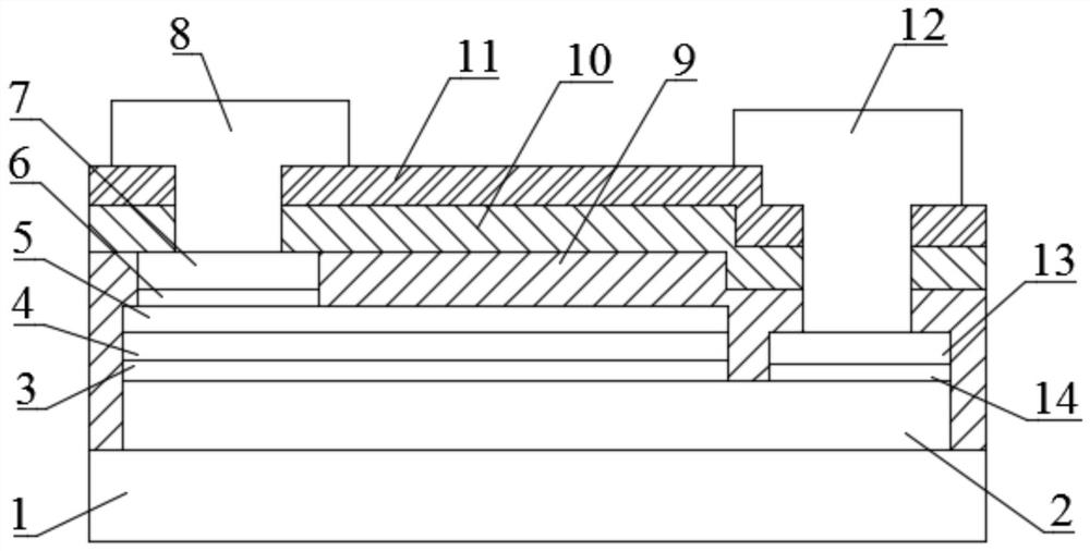
[0060] A Mini LED chip, comprising a substrate layer 1, an N-type gallium nitride layer 2, a multilayer quantum well layer 3, a P-type gallium nitride layer 4, a current spreading layer 5, a P-type contact surface and a current stabilization layer 6, and a P-type gallium nitride layer. Type current injection layer 7, P type welding interface metal layer 8, buffer insulating layer 9, stress release layer 10, insulating full spectrum reflective layer 11, N type welding interface metal layer 12, N type current injection layer 13 and N type Contact surface and current stabilization layer 14.

[0061] Such as figure 1 As shown, the N-type GaN 2 is located in the middle region of the substrate layer 1, and one side of the N-type GaN 2 is sequentially stacked with a multi-layer quantum well layer 3, a P-type GaN layer 4, a current spreading layer 5, The P-type contact surface and current stabilization la...

Embodiment 2

[0067] Please refer to figure 1 , the second embodiment of the present invention is:

[0068] A method for manufacturing a Mini LED chip, comprising the following steps:

[0069] Use lithography equipment and materials such as photolithography machines and photoresists to perform pattern transfer according to the designed chip pattern, use ICP equipment to etch N-type GaN 2 on the middle position of the substrate layer 1, and use N-type GaN on the middle position of the substrate layer 1 On one side of 2, a multilayer quantum well layer 3 and a P-type gallium nitride layer 4 are sequentially fabricated;

[0070] A current spreading layer 5 is fabricated on the P-type gallium nitride layer 4 by means of evaporation. The material of the current spreading layer 5 can be indium tin oxide, indium tungsten oxide or nickel-gold alloy. The engraving facilities and materials are transferred according to the designed chip pattern, and the pattern is etched by chemical etching to obtai...


PUM

PropertyMeasurementUnit
thicknessaaaaaaaaaa
thicknessaaaaaaaaaa

Abstract

The invention discloses a Mini LED chip and a manufacturing method, comprising a GaN substrate, a P-type contact surface and a current stabilization layer, a P-type current injection layer, a P-type welding interface metal layer, a buffer insulating layer, a stress Release layer, insulating full-spectrum reflective layer, N-type welding interface metal layer, N-type current injection layer, N-type contact surface and current stabilization layer; the present invention uses P-type contact surface and current stabilization layer, P-type current injection layer, The use of special functional layers such as buffer insulation layer, stress release layer, N-type current injection layer, N-type contact surface and current stabilization layer solves the problems of current resistance, insulation layer stress, insulation layer adhesion and pad and The problem of the adhesion of the solder paste makes the Mini LED chip have excellent reliability and various performances, and at the same time, it can ensure the production efficiency and production yield of the Mini LED chip.

Description

technical field [0001] The invention relates to the technical field of semiconductor electronics, in particular to a Mini LED chip and a manufacturing method. Background technique [0002] Mini LED chips generally refer to LED chips with a side length between 100 and 200um. Because of their miniaturization, their application fields and manufacturing technology are quite different from traditional LED chips. Mini LEDs are generally used for ultra-high-resolution outdoor large screens, movie screens, and direct-lit backlights for high-end LCD displays. The above three application scenarios cannot be realized by ordinary LEDs. However, due to the small size, complex structure, and extremely high reliability requirements for soldering, temperature resistance, and current resistance, the existing Mini LED chips have problems such as difficult manufacturing, complicated process, and low yield. The reasons for the low rate include but are not limited to insufficient reliability of...

Claims


Application Information

Patent Timeline
Patent Type & Authority Patents(China)
IPC IPC(8): H01L33/06H01L33/12H01L33/14H01L33/36H01L33/44H01L33/46H01L33/00
CPCH01L33/0075H01L33/06H01L33/12H01L33/14H01L33/36H01L33/44H01L33/46
Inventor 张帆
Owner FUJIAN PRIMA OPTOELECTRONICS CO LTD
Why Eureka
Try Eureka