Packaging substrate as well as manufacturing method and packaging structure thereof

A technology for packaging substrates and packaging structures, which is applied in semiconductor/solid-state device manufacturing, electrical components, electric solid-state devices, etc., can solve the problems of poor reliability of joints, influence on overall electrical properties, high cost, etc., and achieve good circuit shape and metal Effects of bump shape, stable package quality, and stable reliability

Active Publication Date: 2011-03-23
UNIMICRON TECH CORP
View PDF0 Cites 9 Cited by
  • Summary
  • Abstract
  • Description
  • Claims
  • Application Information

AI Technical Summary

Problems solved by technology

[0011] Furthermore, the metal bump 22 is arranged on the chip side, which has a higher cost, and since the solder 14 on the package substrate is only a few microns (μm) thick, the contact formed in the application of high I / O count There are often problems with poor adhesion and reliability; in addition, before forming the solder resist layer 12 on the substrate body 10, it is usually necessary to perform a roughening process to improve the bonding between the substrate body 10 and the solder resist layer 12 However, the roughening manufacturing process easily causes deformation of the electrical contact pad 112 and the circuit 111, thereby affecting the overall electrical properties (especially at high frequencies), and will cause difficulties in the electrical connection of the semiconductor chip 20

Method used


Image

  • Packaging substrate as well as manufacturing method and packaging structure thereof
  • Packaging substrate as well as manufacturing method and packaging structure thereof
  • Packaging substrate as well as manufacturing method and packaging structure thereof

Examples


no. 1 example

[0066] see Figure 2A to Figure 2F , is a schematic cross-sectional view of the first embodiment of the packaging substrate, its manufacturing method, and packaging structure of the present invention.

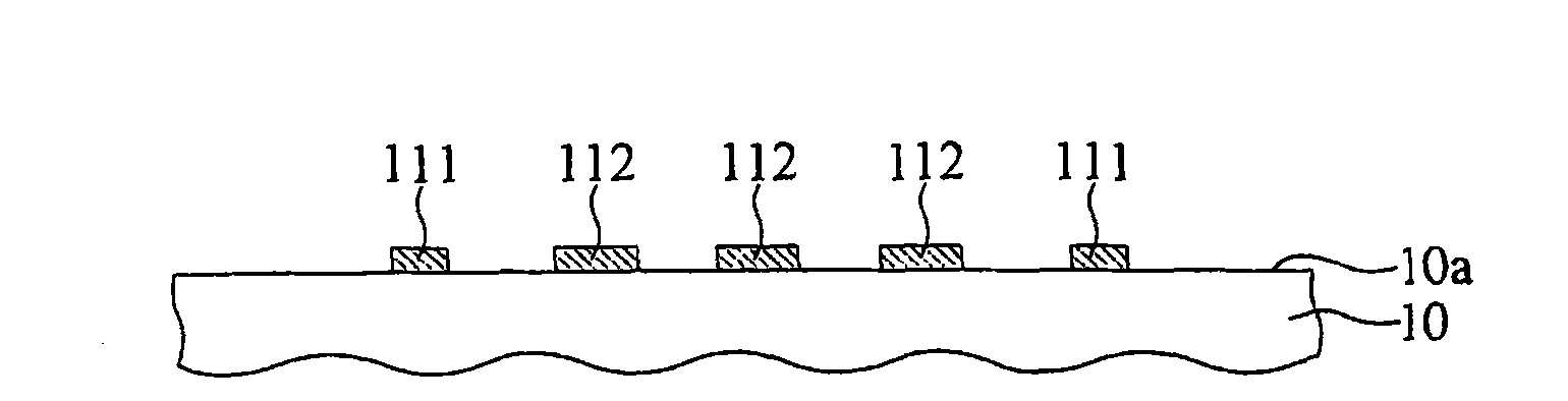
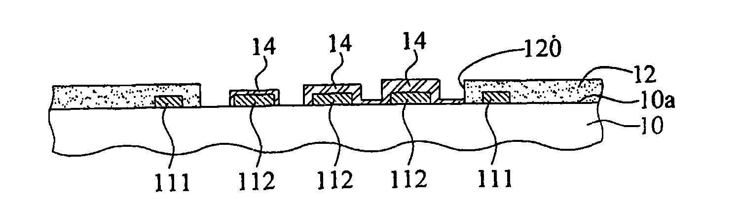
[0067] Such as Figure 2A As shown, first, a substrate body 30 is provided, at least one surface 30 a of which has a plurality of electrical contact pads 312 and circuits 311 , and the electrical contact pads 312 and circuits 311 can be made of copper material.

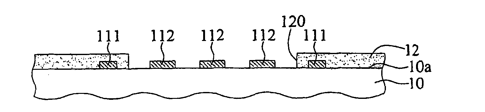
[0068] Such as Figure 2B As shown, an insulating layer 32 is formed on the surface 30a of these electrical contact pads 312, circuits 311 and the substrate body 30, and the thickness of the insulating layer 32 is smaller than the thickness of the electrical contact pads 312 and the circuits 311; Layer 32 can be the organic resin that has good binding force with copper, and the thickness of this insulation layer 32 can be 0.5 to 8 micron (μm) more preferably; In addition, the method for forming this insulation layer ...

no. 2 example

[0080] see Figure 3A to Figure 3H , is a schematic cross-sectional view of a second embodiment of the packaging substrate, its manufacturing method, and packaging structure of the present invention.

[0081] Such as Figure 3A As shown, firstly, a substrate body 50 is provided, at least one surface 50a of which has a conductive layer 51 .

[0082] Such as Figure 3B As shown, a first resistance layer 52 is formed on the conductive layer 51, and the first resistance layer 52 has a plurality of patterned openings 520; then, the conductive layer 51 is used to form lines in these openings 520 by electroplating layer 53, and the circuit layer 53 includes a plurality of electrical contact pads 532 and circuits 531, and the circuit layer 53 can be made of copper material.

[0083] Such as Figure 3C As shown, a second resistive layer 54 is formed on the first resistive layer 52 and the circuit layer 53 , and a plurality of resistive layer openings 540 are formed in the second re...


PUM


Abstract

The invention relates to a packaging substrate as well as a manufacturing method and a packaging structure thereof, providing a substrate body. At least one surface of the substrate body is provided with multiple electric contact pads and lines; insulating layers for covering are formed on the electric contact pads, the lines and the surface of the substrate body; the thickness of the insulating layer is less than the thickness of the electric contact pad; multiple insulating layer open pores correspondingly exposed out of each electric contact pad are formed; a first metal lug is formed on the upper surface exposed out of each electric contact pad so as to be beneficial to the easy control of the welding flux quantity and further beneficial to packaging of thin intervals; a welding preventing layer is not required to be formed on the substrate; and the electric contact pads and the lines are not required to carry out a coursing and manufacturing process so as to maintain a good shape, thus the substrate has good yield and reliability.

Description

technical field [0001] The invention relates to a packaging substrate, its manufacturing method and packaging structure, in particular to a packaging substrate, packaging structure and its manufacturing method which do not need to form a solder mask layer on the substrate. Background technique [0002] In the current flip chip semiconductor packaging technology, a plurality of electrode pads are provided on the semiconductor chip, metal bumps are provided on each of the electrode pads, and a packaging substrate with a plurality of electrical contact pads is provided. , and correspondingly electrically connect the metal bump and the electrical contact pad through solder. [0003] Compared with the traditional wire bonding (Wire Bond) technology, the flip chip technology is characterized in that the electrical connection between the semiconductor chip and the package substrate is made of metal bumps instead of ordinary gold wires, and this flip chip technology The advantage o...

Claims


Application Information

Patent Timeline
Patent Type & Authority Applications(China)
IPC IPC(8): H01L23/498H01L23/48H01L23/12H01L21/48
CPCH01L2224/16225H01L2224/32225H01L2224/73204
Inventor 许诗滨
Owner UNIMICRON TECH CORP
Why Eureka
Try Eureka