Ultraviolet led epitaxy structure and its growth method

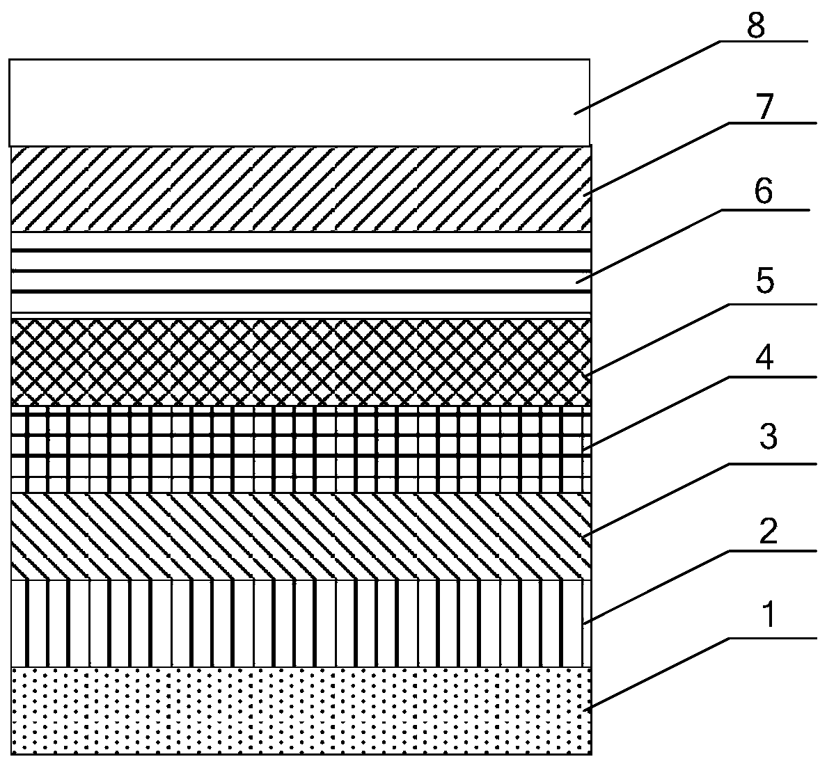
A technology of epitaxial structure and growth method, applied in semiconductor devices, electrical components, circuits, etc., can solve the problems of low current, expansion, P-type layer doping injection efficiency, etc., to reduce impurity scattering, improve efficiency, and improve current. The effect of expanding the ability

Active Publication Date: 2019-07-12
宁波安芯美半导体有限公司
View PDF3 Cites 0 Cited by
  • Summary
  • Abstract
  • Description
  • Claims
  • Application Information

AI Technical Summary

Problems solved by technology

[0005] In view of the shortcomings of the prior art described above, the purpose of the present invention is to provide a method for growing an ultraviolet LED epitaxial structure, which is used to solve the problems of low doping and injection efficiency and current expansion of the P-type layer in the prior art

Method used


Image

  • Ultraviolet led epitaxy structure and its growth method
  • Ultraviolet led epitaxy structure and its growth method

Examples


Embodiment Construction

[0029] Embodiments of the present invention are described below through specific examples, and those skilled in the art can easily understand other advantages and effects of the present invention from the content disclosed in this specification. The present invention can also be implemented or applied through other different specific implementation modes, and various modifications or changes can be made to the details in this specification based on different viewpoints and applications without departing from the spirit of the present invention. It should be noted that, in the case of no conflict, the following embodiments and features in the embodiments can be combined with each other.

[0030] It should be noted that the diagrams provided in the following embodiments are only schematically illustrating the basic ideas of the present invention, although only the components related to the present invention are shown in the diagrams rather than the number, shape and shape of the ...


PUM


Abstract

The invention provides a growth method for an ultraviolet LED epitaxial structure, specially a special growth process for multiple quantum wells of an active area, and the special growth process comprises the following steps: growing LP and PAL as an integral superlattice, wherein a growth period is 5-20; adopting roof type gradual doping for doping of Mg, i.e., gradually reducing after doping ofMg firstly gradually increases to reach a peak value, wherein doping is in symmetrical distribution. Through the superlattice growth, ionization energy of Mg can be reduced, hole concentration is improved, the impurity scattering effect on the hole is reduced, and more holes are injected into a light-emitting area, so that light emitting efficiency is improved. The method is an effective method capable of improving efficiency of an ultraviolet LED; and meanwhile, an apparatus has very good light emitting efficiency, so that photoelectric property of the apparatus is improved.

Description

technical field [0001] The invention relates to the technical field of semiconductor devices, in particular to a growth method of an epitaxial structure capable of increasing hole concentration, increasing hole injection efficiency, improving current spreading capability and ultraviolet LED luminous efficiency, and an epitaxial structure obtained by the method. Background technique [0002] Ultraviolet Light-Emitting Diodes based on III-nitride wide bandgap semiconductor materials have broad application prospects in the fields of sterilization, polymer curing, special lighting, phototherapy, and biochemical detection. . [0003] With the continuous development of LEDs, GaN-based high-brightness LEDs have been commercialized on a large scale, and have shown strong market potential in fields such as landscape lighting, backlight applications, and optical communications. At the same time, the development of white LED solid-state lighting is in full swing, which is triggering t...

Claims


Application Information

Patent Timeline
Patent Type & Authority Patents(China)
IPC IPC(8): H01L33/00H01L33/04H01L33/32
CPCH01L33/005H01L33/04H01L33/32
Inventor 郭丽彬周长健程斌吴礼清
Owner 宁波安芯美半导体有限公司
Why Eureka
Try Eureka