Nitrogen-doped p-type transparent conductive BeZnOS film as well as preparation method and application thereof

A transparent conductive, nitrogen-doped technology, applied in the direction of ion implantation plating, metal material coating process, coating, etc., can solve the problems of low solubility, low N solubility, instability, etc., and achieve simple equipment and operation process, Effect of increasing doping concentration and improving stability

Active Publication Date: 2021-01-08
HUBEI UNIV +1
View PDF7 Cites 0 Cited by
  • Summary
  • Abstract
  • Description
  • Claims
  • Application Information

AI Technical Summary

Problems solved by technology

[0002] At present, the international reports that can be used as p-type ZnO doping elements include group V elements N, P, As, etc., and group I elements Li, Na, etc., among which Li ions have a small radius and are easy to occupy the lattice gap to form donor impurities. It is conducive to the realization of p-type conductivity. Among the group V elements, the size of N atoms is similar to that of O atoms, and the energy level of N acceptors in ZnO is shallow. It has always been considered as the most promising p-type dopant
However, due to the low solubility of N in ZnO and the o unstable, it is difficult to achieve stable p-type conduction
[0003] For the current N-doped ZnO N o It is necessary to improve the problem of unstable acceptor and low solubility of N

Method used


Image

  • Nitrogen-doped p-type transparent conductive BeZnOS film as well as preparation method and application thereof
  • Nitrogen-doped p-type transparent conductive BeZnOS film as well as preparation method and application thereof
  • Nitrogen-doped p-type transparent conductive BeZnOS film as well as preparation method and application thereof

Examples


Embodiment 1

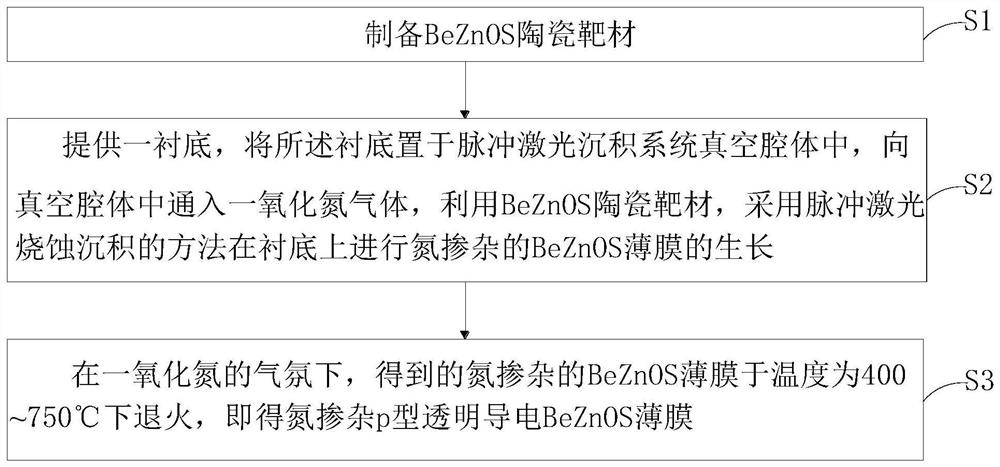
[0033] The invention provides a method for preparing a nitrogen-doped p-type transparent conductive BeZnOS thin film, such as figure 1 shown, including the following steps:

[0034] S1. Preparation of BeZnOS ceramic targets;

[0035] S2. Provide a substrate, place the substrate in the vacuum cavity of the pulsed laser deposition system, pass nitrogen monoxide gas into the vacuum cavity, use the BeZnOS ceramic target material, and adopt the method of pulse laser ablation deposition Nitrogen-doped BeZnOS film growth on the substrate;

[0036] S3. Annealing the obtained nitrogen-doped BeZnOS thin film at a temperature of 400-750° C. in a nitrogen monoxide atmosphere to obtain a nitrogen-doped p-type transparent conductive BeZnOS thin film.

[0037] It should be noted that the preparation method of the BeZnOS ceramic target in the embodiment of the present application includes:

[0038] Weigh ZnS and BeO powders with a molar ratio of 94:6 in a ball mill jar, then add deionized ...

Embodiment 2

[0049] The invention provides a method for preparing a nitrogen-doped p-type transparent conductive BeZnOS thin film, comprising the following steps:

[0050] S1. Preparation of BeZnOS ceramic targets;

[0051] S2. Provide a substrate, place the substrate in the vacuum cavity of the pulsed laser deposition system, pass nitrogen monoxide gas into the vacuum cavity, use the BeZnOS ceramic target material, and adopt the method of pulse laser ablation deposition Nitrogen-doped BeZnOS film growth on the substrate;

[0052] S3. Annealing the obtained nitrogen-doped BeZnOS thin film at a temperature of 400-750° C. in a nitrogen monoxide atmosphere to obtain a nitrogen-doped p-type transparent conductive BeZnOS thin film.

[0053] It should be noted that the preparation method of the BeZnOS ceramic target in the embodiment of the present application includes:

[0054] Weigh ZnS and BeO powders with a molar ratio of 94:6 in a ball mill jar, then add deionized water with 70% of the to...

Embodiment 3

[0064] The invention provides a method for preparing a nitrogen-doped p-type transparent conductive BeZnOS thin film, comprising the following steps:

[0065] S1. Preparation of BeZnOS ceramic targets;

[0066] S2. Provide a substrate, place the substrate in the vacuum cavity of the pulsed laser deposition system, pass nitrogen monoxide gas into the vacuum cavity, use the BeZnOS ceramic target material, and adopt the method of pulse laser ablation deposition Nitrogen-doped BeZnOS film growth on the substrate;

[0067] S3. Annealing the obtained nitrogen-doped BeZnOS thin film at a temperature of 400-750° C. in a nitrogen monoxide atmosphere to obtain a nitrogen-doped p-type transparent conductive BeZnOS thin film.

[0068] It should be noted that the preparation method of the BeZnOS ceramic target in the embodiment of the present application includes:

[0069] Weigh ZnS and BeO powders with a molar ratio of 94:6 in a ball mill jar, then add deionized water with 60% of the to...


PUM

PropertyMeasurementUnit
thicknessaaaaaaaaaa
thicknessaaaaaaaaaa
thicknessaaaaaaaaaa

Abstract

The invention provides a nitrogen-doped p-type transparent conductive BeZnOS film as well as a preparation method and application thereof. The preparation method comprises the following steps of preparing a BeZnOS ceramic target material; providing a substrate, placing the substrate in a vacuum cavity of a pulse laser deposition system, introducing nitric oxide gas into the vacuum cavity, and growing a nitrogen-doped BeZnOS film on the substrate by using a BeZnOS ceramic target material and adopting a pulse laser ablation deposition method; and annealing the obtained nitrogen-doped BeZnOS filmat the temperature of 400-750 DEG C to obtain the nitrogen-doped p-type transparent conductive BeZnOS film. According to the preparation method, Be and S are doped into ZnO to form BeZnOS alloy, an energy band structure and an electronic structure of the BeZnOS alloy can be continuously adjusted, meanwhile, a hexagonal structure of ZnO can be kept, the more stable Be-N bond and the higher valenceband top can reduce the energy level of No, and the stability of No is improved.

Description

technical field [0001] The invention relates to the technical field of p-type transparent conductive thin films, in particular to a nitrogen-doped p-type transparent conductive BeZnOS thin film and its preparation method and application. Background technique [0002] At present, the international reports that can be used as p-type ZnO doping elements include group V elements N, P, As, etc., and group I elements Li, Na, etc., among which Li ions have a small radius and are easy to occupy the lattice gap to form donor impurities. It is conducive to the realization of p-type conductivity. Among the group V elements, the size of N atoms is similar to that of O atoms, and the N acceptor energy level in ZnO is relatively shallow. It has always been considered as the most promising p-type dopant. However, due to the low solubility of N in ZnO and the o unstable, it is difficult to achieve stable p-type conduction. [0003] For the current N-doped ZnO N o It is necessary to impro...

Claims


Application Information

Patent Timeline
Patent Type & Authority Applications(China)
IPC IPC(8): C23C14/06C23C14/28C23C14/58
CPCC23C14/0623C23C14/28C23C14/5806
Inventor 何云斌汪洋黎明锴李磊卢寅梅尹魏玲李派常钢陈俊年尹向阳郭启利李永昌
Owner HUBEI UNIV
Why Eureka
Try Eureka