

Flip-chip camera and manufacturing method thereof
A production method and camera technology, applied in image communication, radiation control devices, television, etc., can solve the problems of difficult production and high cost, and achieve the effects of low production cost, high production efficiency and short connection
Inactive Publication Date: 2019-01-22
江西芯创光电有限公司
View PDF3 Cites 0 Cited by
- Summary
- Abstract
- Description
- Claims
- Application Information
AI Technical Summary
Problems solved by technology
In summary, the purpose of the present invention is to solve the existing camera packaging structure production difficulty, high technical deficiencies, and propose a flip-chip camera and its manufacturing method
Method used
View moreImage
Smart ImageViewing Examples

Examples
Embodiment Construction
Login to View More PUM
 Abstract
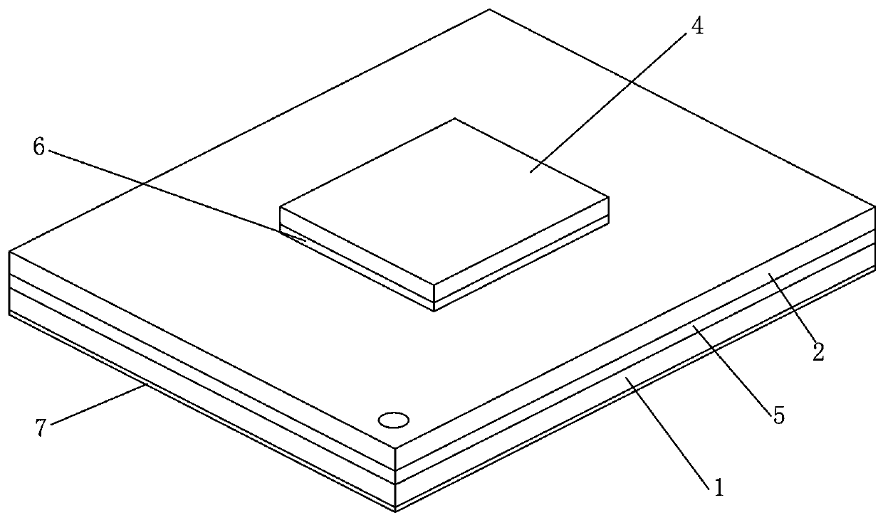
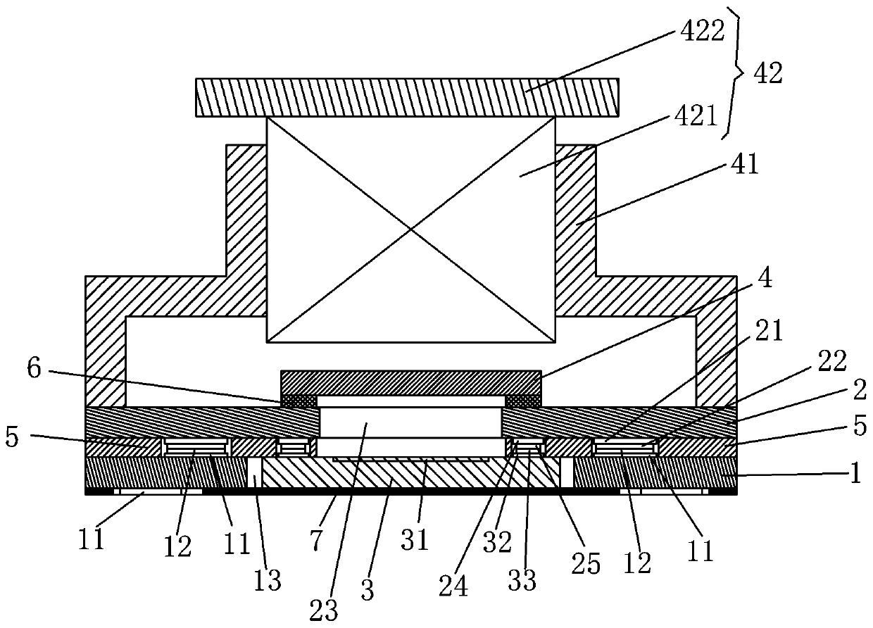
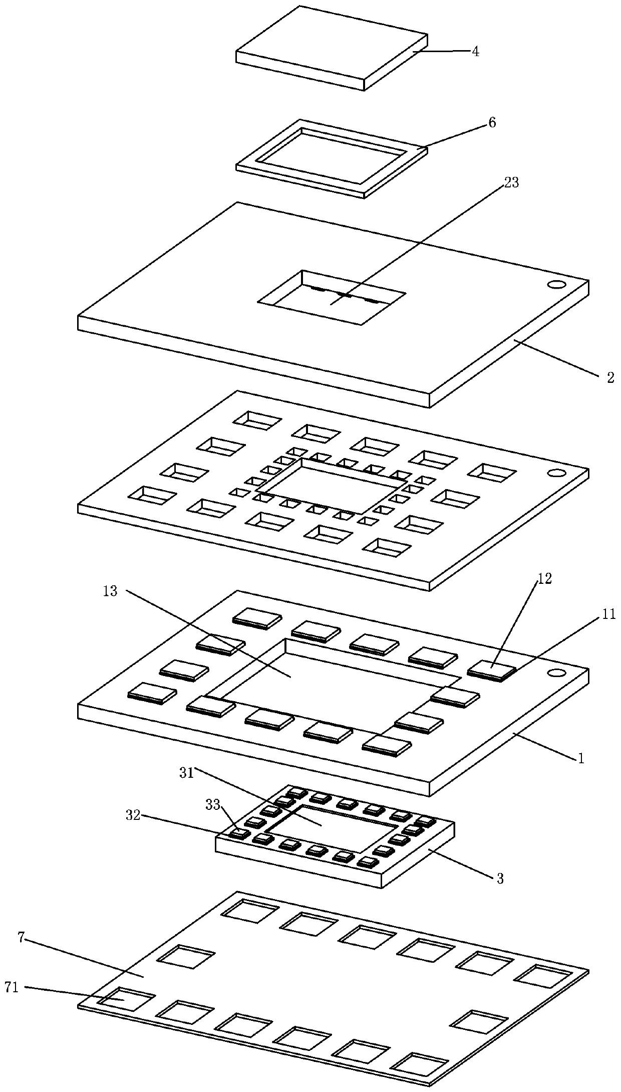
A crystallization camera involves the field of cameras and production methods.There is a difficult and high technical technology with high production and high costs to solve the existing camera packaging structure, including: the first substrate, the second substrate, the camera nude, infrared filter, shell and lens module;The noodle circuit board has the first pads on both sides. The first pad on the front is equipped with the first electrical tile, and the first substrate is equipped with a chip hole that is consistent with the shape of the camera.The camera nude film is the inverted film structure, embedded in the chip hole of the first substrate. The middle part of the front is the sensitivity area, the fourth pad is provided outside the periphery of the sensitivity area, and the fourth pad is provided with a fourth -guide electrical electricity.Blocks; encapsulation of circuit boards and rubber layers, between circuit boards and circuit boards, circuit boards and camera nude films are connected by conductive convex blocks. The packaging process is simple, the production cost is low, and the production efficiency is high.Compared with the traditional COB process overflowing process, it has the advantages of small volume, high performance, and short connection.The trend of the camera is thin and short, and the crystallization method has a good application in this regard.
Description
technical field The invention relates to the technical field of cameras and manufacturing methods. Background technique A camera is a component widely used in the electronics industry. At present, most of the cameras are CSP (Chip Scale Package refers to the chip size package, and its package size is basically the same as the core size of the chip) and COB (Chip On Board, chip-on-board process), and some use flip-chip (flip-chip) Way. CSP is a packaged chip, mostly used for low-end camera chips. However, due to the price and process difficulties in packaging, high-end cameras are mostly shipped as bare chips (die), and then the modules are manufactured by the module factory. At present, most of the module factories around the world use the traditional wire-bond method to make COB modules. The existing common packaging methods generally have technical deficiencies such as high production difficulty and high cost. Contents of the invention To sum up, the purpose of the...
Claims
Login to View More Application Information
Patent Timeline
 Patent Type & AuthorityPatents(China)
IPC IPC(8): H01L27/146H04N5/225
CPCH01L27/14632H01L27/14687H01L27/1469H04N23/50
Inventor陈伟
Owner江西芯创光电有限公司