Rad Hardened Static Random Access Memory

A static random access, radiation hardening technology, applied in static memory, digital memory information, information storage, etc., can solve problems such as poor reliability and radiation particle sensitivity, and achieve improved reliability, small impact on circuit system performance, and small area. and the effect of low power consumption

Inactive Publication Date: 2018-01-23
ZHONGBEI UNIV +1
View PDF3 Cites 1 Cited by
  • Summary
  • Abstract
  • Description
  • Claims
  • Application Information

AI Technical Summary

Problems solved by technology

[0003] The present invention aims to solve the problem that the existing static random access memory is sensitive to radiation particles in space and natural radiation environment, resulting in poor reliability

Method used


Image

  • Rad Hardened Static Random Access Memory
  • Rad Hardened Static Random Access Memory
  • Rad Hardened Static Random Access Memory

Examples


specific Embodiment approach 1

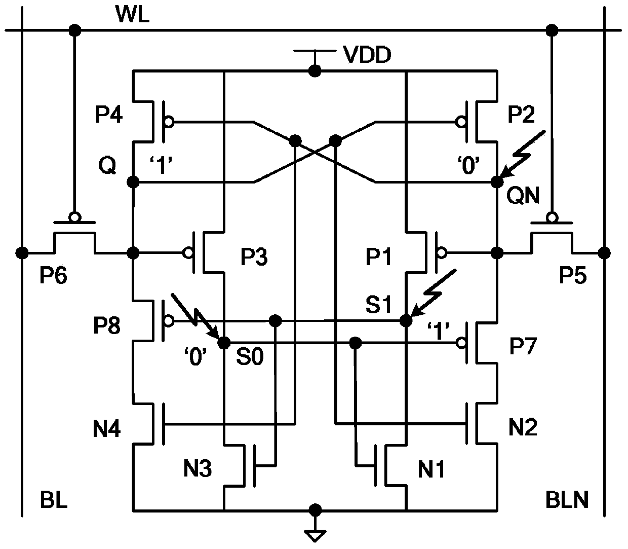
[0021] Specific implementation mode one: refer to figure 1 Describe this embodiment in detail. The anti-radiation hardened static random access memory described in this embodiment includes a No. 1 PMOS transistor P1, a No. 2 PMOS transistor P2, a No. 3 PMOS transistor P3, and a No. 4 PMOS transistor P4. Take the transistor, No. 7 PMOS transistor P7, No. 8 PMOS transistor P8, No. 1 NMOS transistor N1, No. 2 NMOS transistor N2, No. 3 NMOS transistor N3, No. 4 NMOS transistor N4, No. 1 bit line BLN, No. 2 bit line BL and word line WL,

[0022] The access transistors include the fifth PMOS transistor P5 and the sixth PMOS transistor P6,

[0023] The drain of the sixth PMOS transistor P6 is connected to the second bit line BL, and the source of the sixth PMOS transistor P6 is simultaneously connected to the drain of the fourth PMOS transistor P4, the gate of the second PMOS transistor P2, and the gate of the second NMOS transistor N2 The gate of the third PMOS transistor P3 and t...

specific Embodiment approach 2

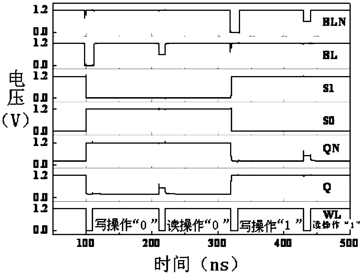
[0045] Embodiment 2: This embodiment is a further description of the anti-radiation hardened SRAM described in Embodiment 1. In this embodiment, when the SRAM is in the storage operation state, the When the line WL is at a high level, the seventh PMOS transistor P7, the fourth PMOS transistor P4, the first PMOS transistor P1, the second NMOS transistor N2 and the third NMOS transistor N3 are all in the on state, and the second PMOS transistor P2 and the third PMOS transistor The transistor P3, the fifth PMOS transistor P5 and the sixth PMOS transistor P6, the first NMOS transistor N1 and the fourth NMOS transistor N4 are all in an off state.

specific Embodiment approach 3

[0046] Specific embodiment three: This embodiment is to further explain the anti-radiation hardened static random access memory described in specific embodiment two. In this embodiment, when the static random access memory is in the read operation state, the first The bit line BLN and the second bit line BL are precharged to the power supply VDD. When the word line WL is at low level, the drain of the sixth PMOS transistor P6 is connected to the drain of the fourth PMOS transistor P4 and the second PMOS transistor P2 The line between the gates of the PMOS transistor P5 and the gate of the fourth PMOS transistor P4 is the node Q, and the node Q maintains the original high level. QN, the node QN is discharged through No. 7 PMOS transistor P7 and No. 2 NMOS transistor N2, and a sense amplifier is used to output the state of the memory according to the voltage difference between the two bit lines to complete the read operation.


PUM


Abstract

The invention relates to a anti-radiation hardened static random access memory, which relates to the field of anti-radiation hardened circuits. The invention aims to solve the problem that the existing static random access memory is sensitive to radiation particles in space and natural radiation environment, resulting in poor reliability. The present invention consists of 12 MOS transistors, which are respectively PMOS transistors P1, P2, P3, P4, P5, P6, P7 and P8 and NMOS transistors N1, N2, N3 and N4. The invention can strengthen the flipping of any single node in the SRAM unit, and can also implement anti-multi-node flipping and fault tolerance for two fixed nodes without depending on the stored value. It is used in integrated circuit design.

Description

technical field [0001] The invention relates to integrated circuit design, in particular to the design of a static random access memory storage unit for anti-single-event reversal effect in the field of anti-radiation hardened circuits. Background technique [0002] With the advancement of integrated circuit technology, Static Random Access Memory (SRAM) has become more sensitive to radiation particles in space and natural radiation environments. The primary particle radiation will cause multiple nodes of the memory cell to flip due to the charge sharing effect, thereby further reducing the reliability of the memory. Therefore, hardened protection against multi-node flipping is required for modern nanomemory. In the present invention, the anti-single event upset (Single Event Upset, SEU) hardening of the SRAM unit is mainly performed by adopting the anti-radiation hardening design (Radiation-Hardening-By-Design, RHBD) technology. Contents of the invention [0003] The in...

Claims


Application Information

Patent Timeline
Patent Type & Authority Patents(China)
IPC IPC(8): G11C11/413
Inventor 郭靖朱磊高金转樊刘华宋瑞佳樊磊刘文怡熊继军
Owner ZHONGBEI UNIV
Why Eureka
Try Eureka